ZHCSGZ9G October 2017 – November 2022 TUSB564
PRODUCTION DATA
- 1 特性
- 2 应用
- 3 说明
- 4 Revision History
- 5 Pin Configuration and Functions
- 6 Specifications
- 7 Parameter Measurement Information
-
8 Detailed Description
- 8.1 Overview
- 8.2 Functional Block Diagram
- 8.3 Feature Description
- 8.4 Device Functional Modes
- 8.5 Programming
- 8.6
Register Maps
- 8.6.1 General Register (address = 0x0A) [reset = 00000001]
- 8.6.2 DisplayPort Control/Status Registers (address = 0x10) [reset = 00000000]
- 8.6.3 DisplayPort Control/Status Registers (address = 0x11) [reset = 00000000]
- 8.6.4 DisplayPort Control/Status Registers (address = 0x12) [reset = 00000000]
- 8.6.5 DisplayPort Control/Status Registers (address = 0x13) [reset = 00000000]
- 8.6.6 USB3.1 Control/Status Registers (address = 0x20) [reset = 00000000]
- 8.6.7 USB3.1 Control/Status Registers (address = 0x21) [reset = 00000000]
- 8.6.8 USB3.1 Control/Status Registers (address = 0x22) [reset = 00000000]
- 9 Application and Implementation
- 10Power Supply Recommendations
- 11Layout
- 12Device and Documentation Support
- 13Mechanical, Packaging, and Orderable Information
7 Parameter Measurement Information
 Figure 7-1 I2C Timing Diagram Definitions
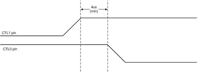 Figure 7-2 USB3.1 to
4-Lane DisplayPort in GPIO Mode
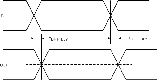 Figure 7-3 Propagation Delay
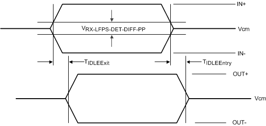 Figure 7-4 Electrical Idle Mode Exit and Entry Delay
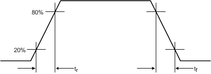 Figure 7-5 Output
Rise and Fall Times
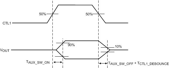 Figure 7-6 AUX and
SBU Switch ON and OFF Timing Diagram