ZHCSGZ9G October 2017 – November 2022 TUSB564
PRODUCTION DATA
- 1 特性
- 2 应用
- 3 说明
- 4 Revision History
- 5 Pin Configuration and Functions
- 6 Specifications
- 7 Parameter Measurement Information
-
8 Detailed Description
- 8.1 Overview
- 8.2 Functional Block Diagram
- 8.3 Feature Description
- 8.4 Device Functional Modes
- 8.5 Programming
- 8.6
Register Maps
- 8.6.1 General Register (address = 0x0A) [reset = 00000001]
- 8.6.2 DisplayPort Control/Status Registers (address = 0x10) [reset = 00000000]
- 8.6.3 DisplayPort Control/Status Registers (address = 0x11) [reset = 00000000]
- 8.6.4 DisplayPort Control/Status Registers (address = 0x12) [reset = 00000000]
- 8.6.5 DisplayPort Control/Status Registers (address = 0x13) [reset = 00000000]
- 8.6.6 USB3.1 Control/Status Registers (address = 0x20) [reset = 00000000]
- 8.6.7 USB3.1 Control/Status Registers (address = 0x21) [reset = 00000000]
- 8.6.8 USB3.1 Control/Status Registers (address = 0x22) [reset = 00000000]
- 9 Application and Implementation
- 10Power Supply Recommendations
- 11Layout
- 12Device and Documentation Support
- 13Mechanical, Packaging, and Orderable Information
9.2.2 Detailed Design Procedure
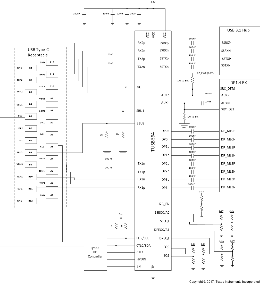
A typical usage of the TUSB564 device is shown in Figure 9-2. The device can be controlled either through its GPIO pins or through its I2C interface. In the example shown below, a Type-C PD controller is used to configure the device through the I2C interface. In I2C mode, the equalization settings for each receiver can be independently controlled through I2C registers. For this reason, the configuration pin CTL1 and all of the equalization pins (EQ[1:0], SSEQ[1:0], and DPEQ[1:0]) can be left unconnected. If these pins are left unconnected, the TUSB564 7-bit I2C target address will be 0x12 because both DPEQ/A1 and SSEQ0/A0 will be at pin level "F". If a different I2C target address is desired, DPEQ/A1 and SSEQ0/A0 pins should be set to a level which produces the desired I2C target address.
 Figure 9-2 Application Circuit