ZHCSH09 October   2017 MSP432E401Y

PRODUCTION DATA.  

  1. 1器件概述
    1. 1.1 特性
    2. 1.2 应用
    3. 1.3 说明
    4. 1.4 功能框图
  2. 2Revision History
  3. 3Device Characteristics
    1. 3.1 Related Products
  4. 4Terminal Configuration and Functions
    1. 4.1 Pin Diagram
    2. 4.2 Pin Attributes
    3. 4.3 Signal Descriptions
      1. Table 4-3 Signal Descriptions
    4. 4.4 GPIO Pin Multiplexing
    5. 4.5 Buffer Type
    6. 4.6 Connections for Unused Pins
  5. 5Specifications
    1. 5.1  Absolute Maximum Ratings
    2. 5.2  ESD Ratings
    3. 5.3  Recommended Operating Conditions
    4. 5.4  Recommended DC Operating Conditions
    5. 5.5  Recommended GPIO Operating Characteristics
    6. 5.6  Recommended Fast GPIO Pad Operating Conditions
    7. 5.7  Recommended Slow GPIO Pad Operating Conditions
    8. 5.8  GPIO Current Restrictions
    9. 5.9  I/O Reliability
    10. 5.10 Current Consumption
    11. 5.11 Peripheral Current Consumption
    12. 5.12 LDO Regulator Characteristics
    13. 5.13 Power Dissipation
    14. 5.14 Thermal Resistance Characteristics, 128-Pin PDT (TQFP) Package
    15. 5.15 Timing and Switching Characteristics
      1. 5.15.1  Load Conditions
      2. 5.15.2  Power Supply Sequencing
        1. 5.15.2.1 Power and Brownout
          1. Table 5-3 Power and Brownout Levels
          2. 5.15.2.1.1 VDDA Levels
          3. 5.15.2.1.2 VDD Levels
          4. 5.15.2.1.3 VDDC Levels
          5. 5.15.2.1.4 VDD Glitch Response
          6. 5.15.2.1.5 VDD Droop Response
      3. 5.15.3  Reset Timing
        1. Table 5-4 Reset Characteristics
      4. 5.15.4  Clock Specifications
        1. 5.15.4.1 PLL Specifications
          1. Table 5-5 Phase Locked Loop (PLL) Characteristics
          2. 5.15.4.1.1 PLL Configuration
        2. 5.15.4.2 PIOSC Specifications
        3. 5.15.4.3 Low-Frequency Oscillator Specifications
          1. Table 5-9 Low-Frequency Oscillator Characteristics
        4. 5.15.4.4 Hibernation Low-Frequency Oscillator Specifications
          1. Table 5-10 Hibernation External Oscillator (XOSC) Input Characteristics
          2. Table 5-11 Hibernation Internal Low-Frequency Oscillator Clock Characteristics
        5. 5.15.4.5 Main Oscillator Specifications
          1. Table 5-12 Main Oscillator Input Characteristics
        6. 5.15.4.6 Main Oscillator Specification WIth ADC
          1. Table 5-14 System Clock Characteristics With ADC Operation
        7. 5.15.4.7 System Clock Characteristics With USB Operation
          1. Table 5-15 System Clock Characteristics With USB Operation
      5. 5.15.5  Sleep Modes
        1. Table 5-16 Wake From Sleep Characteristics
        2. Table 5-17 Wake From Deep Sleep Characteristics
      6. 5.15.6  Hibernation Module
        1. Table 5-18 Hibernation Module Battery Characteristics
        2. Table 5-19 Hibernation Module Characteristics
        3. Table 5-20 Hibernation Module Tamper I/O Characteristics
      7. 5.15.7  Flash Memory
        1. Table 5-21 Flash Memory Characteristics
      8. 5.15.8  EEPROM
        1. Table 5-22 EEPROM Characteristics
      9. 5.15.9  Input/Output Pin Characteristics
        1. Table 5-23 Fast GPIO Module Characteristics
        2. Table 5-24 Slow GPIO Module Characteristics
        3. 5.15.9.1    Types of I/O Pins and ESD Protection
          1. 5.15.9.1.1 Hibernate WAKE pin
            1. Table 5-25 Pad Voltage and Current Characteristics for Hibernate WAKE Pin
          2. 5.15.9.1.2 Nonpower I/O Pins
            1. Table 5-26 Nonpower I/O Pad Voltage and Current Characteristics
      10. 5.15.10 External Peripheral Interface (EPI)
        1. Table 5-28 EPI SDRAM Characteristics
        2. Table 5-29 EPI SDRAM Interface Characteristics
        3. Table 5-30 EPI Host-Bus 8 and Host-Bus 16 Interface Characteristics
        4. Table 5-31 EPI General-Purpose Interface Characteristics
        5. Table 5-32 EPI PSRAM Interface Characteristics
      11. 5.15.11 Analog-to-Digital Converter (ADC)
        1. Table 5-33 Electrical Characteristics for ADC at 1 Msps
        2. Table 5-34 Electrical Characteristics for ADC at 2 Msps
      12. 5.15.12 Synchronous Serial Interface (SSI)
        1. Table 5-35 SSI Characteristics
        2. Table 5-36 Bi- and Quad-SSI Characteristics
      13. 5.15.13 Inter-Integrated Circuit (I2C) Interface
        1. Table 5-37 I2C Characteristics
      14. 5.15.14 Ethernet Controller
        1. 5.15.14.1 DC Characteristics
          1. Table 5-38 Ethernet PHY DC Characteristics
        2. 5.15.14.2 Clock Characteristics for Ethernet
          1. Table 5-39 MOSC 25-MHz Crystal Specification
          2. Table 5-40 MOSC Single-Ended 25-MHz Oscillator Specification
        3. 5.15.14.3 AC Characteristics
          1. Table 5-41 Ethernet Controller Enable and Software Reset Timing
          2. Table 5-42 100Base-TX Transmit Timing
          3. Table 5-43 10Base-T Normal Link Pulse Timing
          4. Table 5-44 Auto-Negotiation Fast Link Pulse (FLP) Timing
          5. Table 5-45 100Base-TX Signal Detect Timing
      15. 5.15.15 Universal Serial Bus (USB) Controller
        1. Table 5-46 ULPI Interface Timing
      16. 5.15.16 Analog Comparator
        1. Table 5-47 Analog Comparator Characteristics
        2. Table 5-48 Analog Comparator Characteristics
        3. Table 5-49 Analog Comparator Voltage Reference Characteristics
        4. Table 5-50 Analog Comparator Voltage Reference Characteristics
      17. 5.15.17 Pulse-Width Modulator (PWM)
        1. Table 5-51 PWM Timing Characteristics
      18. 5.15.18 Emulation and Debug
        1. Table 5-52 JTAG Characteristics
  6. 6Detailed Description
    1. 6.1 Overview
    2. 6.2 Functional Block Diagram
    3. 6.3 Arm Cortex-M4F Processor Core
      1. 6.3.1 Processor Core
      2. 6.3.2 System Timer (SysTick)
      3. 6.3.3 Nested Vectored Interrupt Controller (NVIC)
      4. 6.3.4 System Control Block (SCB)
      5. 6.3.5 Memory Protection Unit (MPU)
      6. 6.3.6 Floating-Point Unit (FPU)
    4. 6.4 On-Chip Memory
      1. 6.4.1 SRAM
      2. 6.4.2 Flash Memory
      3. 6.4.3 ROM
      4. 6.4.4 EEPROM
      5. 6.4.5 Memory Map
    5. 6.5 Peripherals
      1. 6.5.1  External Peripheral Interface (EPI)
      2. 6.5.2  Cyclical Redundancy Check (CRC)
      3. 6.5.3  Advanced Encryption Standard (AES) Accelerator
      4. 6.5.4  Data Encryption Standard (DES) Accelerator
      5. 6.5.5  Secure Hash Algorithm/Message Digest Algorithm (SHA/MD5) Accelerator
      6. 6.5.6  Serial Communications Peripherals
        1. 6.5.6.1 Ethernet MAC and PHY
        2. 6.5.6.2 Controller Area Network (CAN)
        3. 6.5.6.3 Universal Serial Bus (USB)
        4. 6.5.6.4 Universal Asynchronous Receiver/Transmitter (UART)
        5. 6.5.6.5 Inter-Integrated Circuit (I2C)
        6. 6.5.6.6 Quad Synchronous Serial Interface (QSSI)
      7. 6.5.7  System Integration
        1. 6.5.7.1 Direct Memory Access (DMA)
        2. 6.5.7.2 System Control and Clocks
        3. 6.5.7.3 Programmable Timers
        4. 6.5.7.4 Capture Compare PWM (CCP) Pins
        5. 6.5.7.5 Hibernation (HIB) Module
        6. 6.5.7.6 Watchdog Timers
        7. 6.5.7.7 Programmable GPIOs
      8. 6.5.8  Advanced Motion Control
        1. 6.5.8.1 Pulse Width Modulation (PWM)
        2. 6.5.8.2 Quadrature Encoder With Index (QEI) Module
      9. 6.5.9  Analog
        1. 6.5.9.1 ADC
        2. 6.5.9.2 Analog Comparators
      10. 6.5.10 JTAG and Arm Serial Wire Debug
      11. 6.5.11 Peripheral Memory Map
    6. 6.6 Identification
    7. 6.7 Boot Modes
  7. 7Applications, Implementation, and Layout
    1. 7.1 System Design Guidelines
  8. 8器件和文档支持
    1. 8.1 入门和后续步骤
    2. 8.2 器件命名规则
    3. 8.3 工具和软件
    4. 8.4 文档支持
    5. 8.5 Community Resources
    6. 8.6 商标
    7. 8.7 静电放电警告
    8. 8.8 出口管制提示
    9. 8.9 术语表
  9. 9机械、封装和可订购信息

VDDA Levels

The VDDA supply has three monitors:

  • Power-on reset (POR)
  • Power-OK (POK)
  • Brownout reset (BOR)

The POR monitor is used to keep the analog circuitry in reset until the VDDA supply reaches the correct range for the analog circuitry to begin operating. The POK monitor is used to keep the digital circuitry in reset until the VDDA power supply is at an acceptable operational level. The digital reset is only released when the Power-On Reset has deasserted and the Power-OK monitor for each supply indicates that power levels are in operational ranges. The BOR monitor is used to generate a reset to the device or assert an interrupt if the VDDA supply drops below its operational range.

NOTE

VDDA BOR and VDD BOR events are a combined BOR to the system logic, such that if either BOR event occurs, the following bits are affected:

  • The BORRIS bit in the Raw Interrupt Status (RIS) register, System Control offset 0x050
  • The BORMIS bit in the Masked Interrupt Status and Clear (MISC) register, System Control offset 0x058. This bit is set only if the BORIM bit in the Interrupt Mask Control (IMC) register has been set.
  • The BOR bit in the Reset Cause (RESC) register, System Control offset 0x05C. This bit is set only if either of the BOR events have been configured to initiate a reset.

In addition, the following bits control both BOR events:

  • The BORIM bit in the Interrupt Mask Control (IMC) register, System Control offset 0x054
  • The VDDA_UBOR0 and VDD_UBOR0 bits in the Power-Temperature Cause (PWRTC) register

See the System Control chapter of the MSP432E4 SimpleLink™ Microcontrollers Technical Reference Manual for more information on how to configure these registers.

Figure 5-2 shows the relationship between VDDA, POK, POR, and a BOR event.
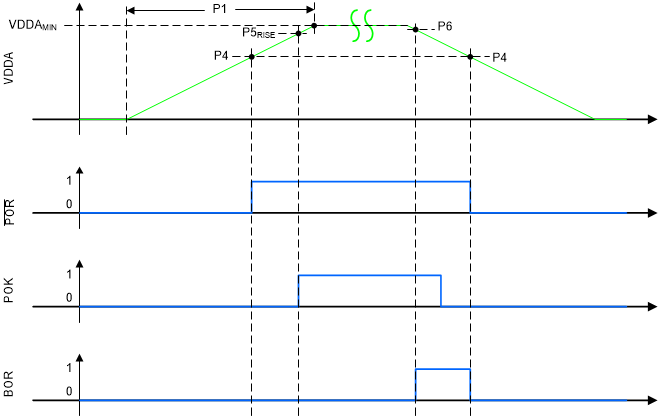
MSP432E401Y Snowflake_A0_VDDA_POK.gifFigure 5-2 Power and Brownout Assertions vs VDDA Levels