ZHCSH16C November 2017 – August 2019 TPS25820 , TPS25821
PRODUCTION DATA.
- 1 特性
- 2 应用
- 3 说明
- 4 修订历史记录
- 5 Pin Configuration and Functions
- 6 Specifications
- 7 Detailed Description
-
8 Application and Implementation
- 8.1 Application Information
- 8.2 Typical Applications
- 9 Power Supply Recommendations
- 10Layout
- 11器件和文档支持
- 12机械、封装和可订购信息
6.6 Switching Characteristics
–40°C ≤ TJ ≤ 125°C, 4.5 V ≤ VIN ≤ 5.5 V, VEN = VCHG = VIN, RREF = 100 kΩ. Typical values are at 25°C. All voltages are with respect to GND. IOUT and IOS defined positive out of the indicated pin (unless otherwise noted)| PARAMETER | TEST CONDITIONS | MIN | TYP | MAX | UNIT | |
|---|---|---|---|---|---|---|
| OUT - POWER SWITCH | ||||||
| tr | Output voltage rise time | VIN = 5 V, CL = 1 µF, RL = 100 Ω (measure between 10% and 90% of final value) | 0.5 | 0.8 | 1.2 | ms |
| tf | Output voltage fall time | 0.2 | 0.3 | 0.4 | ms | |
| ton | Output voltage turn-on time | VIN = 5 V, CL = 1 µF, RL = 100 Ω | 2.1 | 3.2 | 4.5 | ms |
| toff | Output voltage turn-off time | 0.8 | 1.3 | 1.9 | ms | |
| tw_OUT_DCHG | RDCHG application time at OUT turn off | VOUT = 1 V, time ISNK_OUT > 1 mA after Sink termination removed from CC lines | 169 | 262 | 361 | ms |
| OUT - CURRENT LIMIT | ||||||
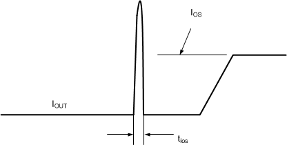
| tiOS | Current limit response time to short circuit | VIN - VOUT = 1 V, RL = 10 mΩ (see Figure 1) | 1.5 | 4 | µs | |
| FAULT | ||||||
| tDEGA | Asserting deglitch due to overcurrent | 5.6 | 8.2 | 10.6 | ms | |
| tDEGA | Asserting deglitch due to overtemperature in current limit | 0 | ms | |||
| tDEGD | De-asserting deglitch | 5.6 | 8.2 | 10.6 | ms | |
| CC1/CC2 - VCONN POWER SWITCH (TPS25820) | ||||||
| tr | Output voltage rise time | VIN2 = 5 V, CL = 1 µF, RL = 100 Ω | 0.13 | 0.22 | 0.3 | ms |
| tf | Output voltage fall time | 0.18 | 0.22 | 0.26 | ms | |
| ton | Output voltage turn-on time | VIN2 = 5 V, CL = 1 µF, RL = 100 Ω | 1.4 | 2.2 | 3.2 | ms |
| toff | Output voltage turn-off time | 0.25 | 0.33 | 0.4 | ms | |
| Minimum VCONN discharge time | TPS25820 | 42 | 65 | 90 | ms | |
| CC1/CC2 - VCONN POWER SWITCH - CURRENT LIMIT (TPS25820) | ||||||
| tres | Current limit response time to short circuit | VIN – VCCx = 1 V, R = 10 mΩ (see Figure 1) | 1 | 4 | µs | |
| SINK, POL | ||||||
| tDEGA | Asserting deglitch | 100 | 150 | 200 | ms | |
| tDEGD | De-asserting deglitch | 7.9 | 12.5 | 17.7 | ms | |
 Figure 1. Output Short Circuit Parameter Diagram