ZHCSH20 October 2017 TAS5634
PRODUCTION DATA.
- 1 特性
- 2 应用
- 3 说明
- 4 修订历史记录
- 5 Device Comparison
- 6 Pin Configuration and Functions
- 7 Specifications
-
8 Detailed Description
- 8.1 Overview
- 8.2 Functional Block Diagrams
- 8.3
Feature Description
- 8.3.1 Closed-Loop Architecture
- 8.3.2 Power Supplies
- 8.3.3 System Power-Up / Power-Down Sequence
- 8.3.4 Startup and Shutdown Ramp Sequence (C_START)
- 8.3.5 Device Protection System
- 8.3.6 Overload and Short Circuit Current Protection
- 8.3.7 DC Speaker Protection
- 8.3.8 Pin-To-Pin Short Circuit Protection (PPSC)
- 8.3.9 Overtemperature Protection
- 8.3.10 Overtemperature Warning, OTW
- 8.3.11 Undervoltage Protection (UVP) and Power-On Reset (POR)
- 8.3.12 Error Reporting
- 8.3.13 Fault Handling
- 8.3.14 System Design Consideration
- 8.4 Device Functional Modes
- 9 Application and Implementation
- 10Power Supply Recommendations
- 11Layout
- 12器件和文档支持
- 13机械、封装和可订购信息
8 Detailed Description
8.1 Overview
The TAS5634 is a PWM Input, Class-D Audio amplifier power stage that can be paired with TI digital-input PWM modulator like the TAS5548 or TAS5558. The TAS5634 supports up to 58V on the output stage power supply (PVDD) to deliver up to 2 x 300 W (6Ω) or 1 x 600 W (3Ω) for higher impedance loads. The output of the TAS5634 can be configured in single-ended (SE), bridge-tied load (BTL) or parallel bridge-tied load (PBTL) output, which supports 4-channels, stereo, or mono, respectively. It requires two power supply rails for operation, PVDD for the output power stage and 12 V for the gate drive (GVDD) and internal circuitry (VDD). Figure 19 shows typical connections for BTL outputs. A detailed schematic can be viewed in TAS5634EVM User's Guide.
8.2 Functional Block Diagrams
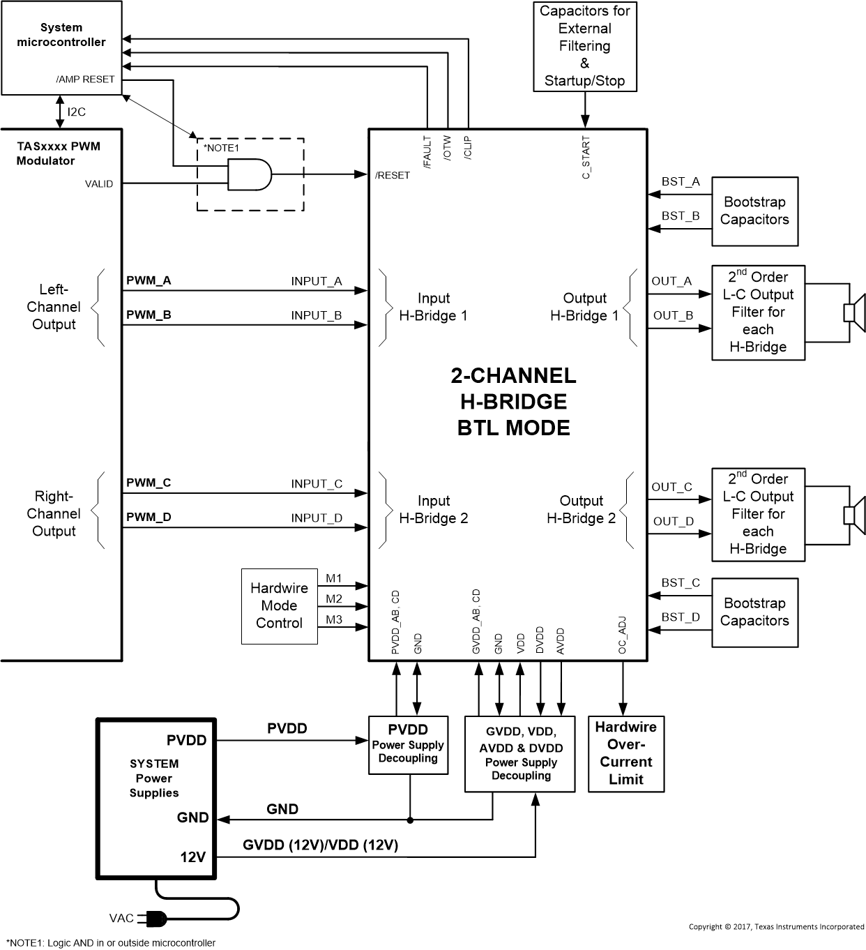
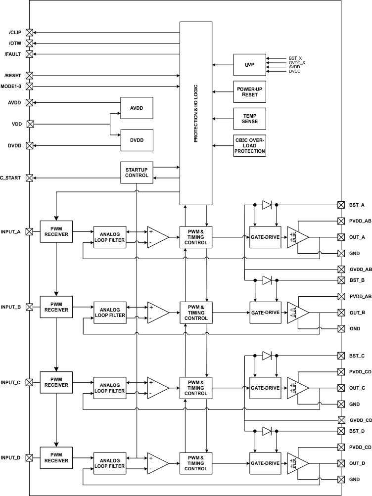 Figure 20. Functional Block Diagram
8.3 Feature Description
8.3.1 Closed-Loop Architecture
The TAS5634 is designed with closed-loop feedback to reduce noise and eliminate distortion caused by the power supply and output stage FETs. The integrated closed-loop architecture makes it simple and easy to convert from an audio digital source directly to power delivery in one step while maintaining great performance.
8.3.2 Power Supplies
The TAS5634 requires only two supplies for normal operation including a high-voltage output stage supply, PVDD, and a lower voltage 12V voltage supply for gate drive and low-voltage analog and digital circuits. Two internal regulators provide voltage regulation for the digital (DVDD) and analog (AVDD) circuit using the 12V VDD voltage supply. Additionally, an integrated bootstrap (floating) supply provides the necessary voltage for the high-side MOSFETs for each half-bridge.
To provide the best electrical and acoustical characteristics, the PWM signal path including gate drive and output stage are designed as identical, independent half-bridges. For this reason, each half-bridge has separate bootstrap pins (BST_X) and each full-bridge has separate power stage supply (PVDD_X) and gate supply (GVDD_X) pins.
Special attention should be paid to the power-stage power supply; this includes component selection, PCB placement, and routing. As indicated, each full-bridge has independent power-stage supply pins (PVDD_X). For optimal electrical performance, EMI compliance, and system reliability, it is important that each PVDD_X connection is decoupled with a minimum of 470 nF ceramic capacitance and placed as close as possible to each supply pin. It is recommended to follow the PCB layout of the TAS5634 reference design. For additional information on recommended power supply and required components, see the application diagrams in this data sheet.
The power-supply sequence is not critical because of the internal power-on-reset circuit. The TAS5634 is fully protected against erroneous power-stage turn on due to parasitic gate charging when power supplies are applied. Thus, voltage-supply ramp rates (dV/dt) are non-critical within the specified range (see the Recommended Operating Conditions table of this data sheet).
8.3.2.1 BST, Bootstrap Supply
The TAS5634 uses bootstrap circuits to properly turn on the high-side MOSFETs. A small ceramic capacitor must be connected from each bootstrap pin (BST_X) to the power-stage output pin (OUT_X). When the power-stage output is low, the bootstrap capacitor is charged through an internal diode connected between the gate-drive power-supply pin (GVDD_X) and the bootstrap pin (BST_X). When the power-stage output is high, the bootstrap capacitor potential is shifted above the output potential and thus provides a suitable voltage supply for the high-side gate driver. In an application with PWM switching frequencies in the range from 352kHz to 500 kHz, it is recommended to use 33 nF ceramic capacitors, size 0603 or 0805, for the bootstrap supply. These 33-nF capacitors ensure sufficient energy storage, even during minimal PWM duty cycles, to keep the high-side power stage MOSFETs fully turned on during the remaining part of the PWM cycle.
8.3.2.2 PVDD, Output Stage Power Supply
The PVDD_x voltage pins supply the high voltage and current needed for driving the speaker load.
- Place at least 1 μF decoupling capacitance as close as possible to each supply pin, PVDD_AB and PVDD_CD. TI recommends to use ceramic capacitors, which have low series resistance (ESR). The decoupling capacitors provide current each output stage switch cycle.
- Add a minimum of 470 μF bulk capacitance to each PVDD_x pin. More capacitance may be required if the power supply has low bandwidth or does not respond quickly to transients.
- Minimize trace lengths between decoupling and bulk capacitance to reduce inductance between the TAS5634 and the supply capacitors.
8.3.2.3 GVDD, Gate-Drive Power Supply
The GVDD_x, 12 V power supply is required for the gate-drive section of the TAS5634. Place a minimum of 100 nF decoupling capacitor near each GVDD_x pin. For best audio performance, place a total of 10 μF bulk capacitance on the 12V power supply.
8.3.2.4 VDD Supply, Internal Regulators (DVDD and AVDD)
The TAS5634 has two internal regulators, which are used to power the low voltage digital (DVDD) and analog (AVDD) circuitry. The 12V VDD pin can be supplied from the same power supply as GVDD_x. For best audio performance, separate VDD from GVDD_AB and GVDD_CD using RC filters. The RC filters will provide high-frequency isolation and minimize the amount of switching noise on DVDD and AVDD.
8.3.3 System Power-Up / Power-Down Sequence
8.3.3.1 Powering Up
The TAS5634 does not require a power-up sequence. The outputs of the H-bridges remain in a high-impedance state until the gate-drive supply voltage (GVDD_X) and VDD voltage are above the undervoltage protection (UVP) voltage threshold (see the Electrical Characteristics table of this data sheet). Although not specifically required, it is recommended to hold RESET in a low state while powering up the device. This allows an internal circuit to charge the external bootstrap capacitors by enabling a weak pulldown of the half-bridge output.
8.3.3.2 Powering Down
The TAS5634 does not require a power-down sequence. The device remains fully operational as long as the gate-drive supply (GVDD_X) voltage and VDD voltage are above the undervoltage protection (UVP) voltage threshold (see the Electrical Characteristics table of this data sheet). Although not specifically required, it is a good practice to hold RESET low during power down, thus preventing audible artifacts including pops or clicks.
8.3.4 Startup and Shutdown Ramp Sequence (C_START)
The integrated startup and stop sequence ensures a click and pop free startup and shutdown sequence of the amplifier. The startup sequence uses a voltage ramp with a duration set by the CSTART capacitor. The sequence uses the input PWM signals to generate output PWM signals, hence input idle PWM should be present during both startup and shut down ramping sequences.
VDD, GVDD_X and PVDD_X power supplies must be turned on and with settled outputs before starting
the startup ramp by setting RESET high.
During startup and shutdown ramp the input PWM signals should be in muted condition with the PWM processor noise shaper activity turned off (50% duty cycle).
The duration of the startup and shutdown ramp is 100 ms + X ms, where X is the CSTART capacitor value in nF. It is recommended to use 330 nF CSTART in BTL and PBTL mode and 1 µF in SE mode configuration. This results in ramp times of 430 ms and 1.1 s respectively. The longer ramp time in SE configuration allows charge and discharge of the output AC coupling capacitor without audible artifacts. See the for a complete list of recommended C_START values.
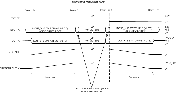 Figure 21. Start-Up and Shutdown Ramp
8.3.5 Device Protection System
The TAS5634 contains advanced protection circuitry carefully designed to facilitate system integration and ease of use, as well as to safeguard the device from permanent failure due to a wide range of fault conditions such as short circuits, overload, overtemperature, and undervoltage. The TAS5634 responds to a fault by immediately setting the power stage in a high-impedance (Hi-Z) state and asserting the FAULT pin low. In situations other than overload and overtemperature error (OTE), the device automatically recovers when the fault condition has been removed, i.e., the supply voltage has increased.
The device will function on errors, as shown in the following table.
Table 2. Device Protection
| BTL Mode | SE Mode | ||
|---|---|---|---|
| Channel Fault | Turns Off | Channel Fault | Turns Off |
| A | A+B | A | A+B |
| B | B | ||
| C | C+D | C | C+D |
| D | D | ||
Bootstrap UVP does not shutdown according to the table, it shuts down the respective high-side FET.
8.3.6 Overload and Short Circuit Current Protection
TAS5634 has fast reacting current sensors with a programmable trip threshold (OC threshold) on all high-side and low-side FETs. To prevent output current to increase beyond the programmed threshold, TAS5634 has the option of either limiting the output current for each switching cycle (Cycle By Cycle Current Control, CB3C) or to perform an immediate shutdown of the output in case of excess output current (Latching Shutdown). CB3C prevents premature shutdown due to high output current transients caused by high level music transients and a drop of real speaker’s load impedance, and will allow the output current to be limited to a maximum programmed level. If the maximum output current persists, i.e. the power stage being overloaded with too low load impedance, the device will shut down the affected output channel and the affected output will be put in a high-impedance (Hi-Z) state until a /RESET cycle is initiated. CB3C works individually for each half bridge output. If an over current event is triggered, CB3C will perform a state flip of the half bridge output that will be cleared upon beginning of next PWM frame.
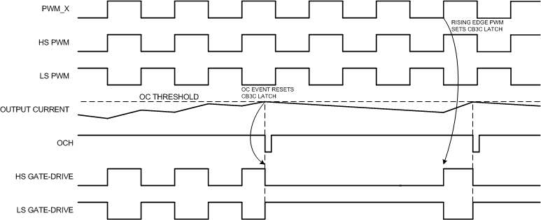 Figure 22. CB3C Timing Example
During CB3C an over load counter will increment for each over current event and decrease for each non-over current PWM cycle. This allows full amplitude transients into a low speaker impedance without a shutdown protection action. In case of a short circuit condition, the over current protection will limit the output current by the CB3C operation and eventually shut down the affected output if the overload counter reaches its maximum value. If a latched OC operation is required such that the device will shut down the affected output immediately upon first detected over current event, this protection mode should be selected.
The over current threshold and mode (CB3C or Latched OC) is programmed by the OC_ADJ resistor value. The OC_ADJ resistor needs to be within its intentional value range for either CB3C operation or Latched OC operation.
 Figure 23. OC Threshold versus OC_ADJ Resistor Value Example
Table 3. OC_ADJ Resistor Value for OC Threshold
| OC_ADJ Resistor Value | Protection Mode | OC Threshold |
|---|---|---|
| 24 kΩ | CB3C | 15.5 A |
| 27 kΩ (Typ) | CB3C | 14 A |
| 30 kΩ | CB3C | 13 A |
| 33 kΩ | CB3C | 12 A |
| 47 kΩ | Latched OC | 15.5 A |
| 56 kΩ (Typ) | Latched OC | 14 A |
| 68 kΩ | Latched OC | 13 A |
| 62 kΩ | Latched OC | 12 A |
TI recommends to use a 27kΩ (CB3C) or 56kΩ (Latched) overcurrent adjust resistor value for typical applications. When using 24 kΩ (CB3C) or 47 kΩ (Latched) OC_ADJ resistor values, layout is critical for device reliability due to increased current during overcurrent events. Please carefully follow the guidelines in section Printed Circuit Board Requirements and only use these resistor values if required to deliver the desired power to the load.
8.3.7 DC Speaker Protection
The output DC protection scheme protects a connected speaker from excess DC current caused by a speaker wire accidentally shorted to chassis ground. Such short circuit would result in a DC voltage of PVDD/2 across the speaker, which potentially can result in destructive current levels. The output DC protection detects any unbalance of the output and input current of a BTL output, and in case of the unbalance exceeding a programmed threshold, the overload counter will increment until its maximum value and the affected output channel will be shut down. Output DC protection is designed for use in BTL configuration with AD mode modulation, and should be disabled if BD mode operation is used due to the output filter inductors’ ripple currents being in phase in BD mode and will thus be counted as an unbalanced current. DC Speaker Protection can be disabled for BTL operation with BD mode modulation, see Mode Setup Table for configuration.
8.3.8 Pin-To-Pin Short Circuit Protection (PPSC)
The PPSC detection system protects the device from permanent damage if a power output pin (OUT_X) is shorted to GND or PVDD_X. For comparison, the OC protection system detects an over current after the demodulation filter where PPSC detects shorts directly at the pin before the filter. PPSC detection is performed at startup i.e. when VDD is supplied, consequently a short to either GND or PVDD_X after system startup will not activate the PPSC detection system. When PPSC detection is activated by a short on the output, all half bridges are kept in a Hi-Z state until the short is removed, the device then continues the startup sequence and starts switching. The detection is controlled globally by a two step sequence. The first step ensures that there are no shorts from OUT_X to GND, the second step tests that there are no shorts from OUT_X to PVDD_X. The total duration of this process is roughly proportional to the capacitance of the output LC filter. The typical duration is <15 ms/μF. While the PPSC detection is in progress, FAULT is kept low, and the device will not react to changes applied to the RESET pins. If no shorts are present the PPSC detection passes, and FAULT is released. A device reset will not start a new PPSC detection. PPSC detection is enabled in BTL output configuration, the detection is not performed in SE mode. To make sure not to trip the PPSC detection system it is recommended not to insert resistive load to GND or PVDD_X.
8.3.9 Overtemperature Protection
The TAS5634 has a two-level temperature-protection system that asserts an active-low warning signal (OTW) when the device junction temperature exceeds 125°C (typical). If the device junction temperature exceeds 155°C (typical), the device is put into thermal shutdown, resulting in all half-bridge outputs being set in the high-impedance (Hi-Z) state and FAULT being asserted low. OTE is latched in this case. To clear the OTE latch, RESET must be asserted. Thereafter, the device resumes normal operation.
8.3.10 Overtemperature Warning, OTW
The over temperature warning OTW asserts when the junction temperature has exceeded recommended operating temperature. Operation at junction temperatures above OTW threshold is exceeding recommended operation conditions and is strongly advised to avoid.
If OTW asserts, action should be taken to reduce power dissipation to allow junction temperature to decrease until it gets below the OTW hysteresis threshold. This action can be decreasing audio volume or turning on a system cooling fan.
8.3.11 Undervoltage Protection (UVP) and Power-On Reset (POR)
The UVP and POR circuits of the TAS5634 fully protect the device in any power-up/down and brownout situation. While powering up, the POR circuit resets the overload circuit (OLP) and ensures that all circuits are fully operational when the GVDD_X and VDD supply voltages reach stated in the Electrical Characteristics table. Although GVDD_X and VDD are independently monitored, a supply voltage drop below the UVP threshold on any VDD or GVDD_X pin results in all half-bridge outputs immediately being set in the high-impedance (Hi-Z) state and FAULT being asserted low. The device automatically resumes operation when all supply voltages have increased above the UVP threshold.
8.3.12 Error Reporting
Note that asserting RESET low forces the FAULT signal high, independent of faults being present. TI recommends monitoring the OTW signal using the system micro controller and responding to an overtemperature warning signal by, e.g., turning down the volume to prevent further heating of the device resulting in device shutdown (OTE).
To reduce external component count, an internal pullup resistor to 3.3 V is provided on FAULT, CLIP, and OTW outputs. See Electrical Characteristics table for actual values.
The FAULT, OTW, pins are active-low, open-drain outputs. Their function is for protection-mode signaling to a PWM controller or other system-control device.
Any fault resulting in device shutdown is signaled by the FAULT pin going low. Likewise, OTW goes low when the device junction temperature exceeds 125°C (see Table 4).
Table 4. Error Reporting
| FAULT | OTW | DESCRIPTION | |
|---|---|---|---|
| 0 | 0 | Overtemperature (OTE) or overload (OLP) or undervoltage (UVP) | |
| 0 | 1 | Overload (OLP) or undervoltage (UVP) | |
| 1 | 0 | Junction temperature higher than 125°C (overtemperature warning) | |
| 1 | 1 | Junction temperature lower than 125°C and no OLP or UVP faults (normal operation) | |
8.3.13 Fault Handling
If a fault situation occurs while in operation, the device will act accordingly to the fault being a global or a channel fault. A global fault is a chip-wide fault situation and will cause all PWM activity of the device to be shut down, and will assert FAULT low. A global fault is a latching fault and clearing FAULT and restart operation requires resetting the device by toggling RESET. Toggling RESET should never be allowed with excessive system temperature, so it is advised to monitor RESET by a system microcontroller and only allow releasing RESET (RESET high) if the OTW signal is cleared (high). A channel fault will result in shutdown of the PWM activity of the affected channel(s). Note that asserting RESET low forces the FAULT signal high, independent of faults being present. TI recommends monitoring the OTW signal using the system micro controller and responding to an over temperature warning signal by, that is, turning down the volume to prevent further heating of the device resulting in device shutdown (OTE).
Table 5. Fault Handling
| Fault/Event | Fault/Event Description |
Global or Channel |
Reporting Method | Latched/Self Clearing | Action needed to Clear | Output FETs |
|---|---|---|---|---|---|---|
| PVDD_X UVP | Voltage Fault | Global | FAULT Pin | Self Clearing | Increase affected supply voltage | Hi-Z |
| VDD UVP | ||||||
| GVDD_X UVP | ||||||
| AVDD UVP | ||||||
| POR (DVDD UVP) | Power On Reset | Global | FAULT Pin | Self Clearing | Allow DVDD to rise | H-Z |
| BST UVP | Voltage Fault | Channel (half bridge) | None | Self Clearing | Allow BST cap to recharge (lowside on, VDD 12V) |
High-side Off |
| OTW | Thermal Warning | Global | OTW Pin | Self Clearing | Cool below lower OTW threshold | Normal operation |
| OTE (OTSD) | Thermal Shutdown | Global | FAULT Pin | Latched | Toggle RESET | Hi-Z |
| OLP (CB3C >2.6 ms) | OC shutdown | Channel | FAULT Pin | Latched | Toggle RESET | Hi-Z |
| Latched OC (ROC > 47 k) |
OC shutdown | Channel | FAULT Pin | Latched | Toggle RESET | Hi-Z |
| CB3C (24k < ROC < 33k) |
OC Limiting | Channel | None | Self Clearing | Reduce signal level or remove short | Flip state, cycle by cycle at fs/2 |
| Stuck at Fault(1) (1 to 3 channels) | No PWM | Channel | None | Self Clearing | Resume PWM | Hi-Z |
| Stuck at Fault(1) (All channels) | No PWM | Global | None | Self Clearing | Resume PWM | Hi-Z |
8.3.14 System Design Consideration
A rising-edge transition on RESET input allows the device to execute the startup sequence and starts switching.
Apply audio only according to the timing information for startup and shutdown sequence. That will start and stop the amplifier without audible artifacts in the output transducers.
The CLIP signal indicates that the output is approaching clipping (when output PWM starts skipping pulses due to loop filter saturation). The signal can be used to initiate an audio volume decrease or to adjust the power supply rail.
The device inverts the audio signal from input to output.
The DVDD and AVDD pins are not recommended to be used as a voltage source for external circuitry.
8.4 Device Functional Modes
There are three main output modes supported on the TAS5634 including stereo BTL mode, mono PBTL mode and 4-channel single-ended mode. In addition, a combination of one BTL channel and two SE channels for a 2.1 system can also be selected. The device supports two PWM modulation modes, AD and BD. AD modulation mode supports single-ended (SE) or differential PWM inputs. AD modulation can also be configured to have SE, BTL, BTL + SE, or PBTL outputs. BD modulation requires differential PWM inputs. BD modulation can only be configured in BTL or PBTL mode.
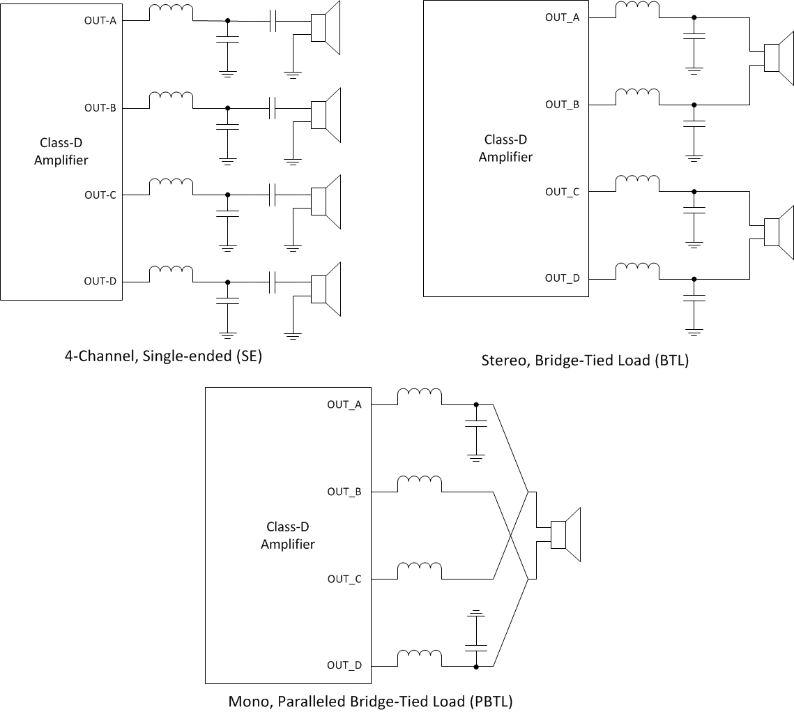 Figure 24. Device Functional Modes Configurations
8.4.1 Stereo, Bridge-tied Load (BTL)
In bridge-tied load (BTL) mode, the device operates as a 2-channel, stereo amplifier. BTL uses two of the output stage half-bridges to product up to twice PVDD across the load. BTL mode has a few configuration options:
- AD or BD Modulation
- Single-ended (AD) or Differential Input (AD or BD)
- DC Speaker Protection in AD modulation mode
When using the singled-ended input configuration, the input signal is converted to a differential signal to drive the output stage of the TAS5634.
See Table 1. Mode Selection Pins for the appropriate pin configurations and section Typical BTL Application for specific application setup information.
8.4.2 Mono, Paralleled Bridge-tied Load (PBTL)
In parallel bridge-tied load (PBTL) mode, the device operates as a 1-channel, mono amplifier. PBTL is typically used for 3 Ω and 4 Ω impedances delivering up to twice the current compared with the BTL configuration. PBTL configuration options include:
- AD or BD Modulation
- Single-ended (AD) or Differential Input (AD or BD)
- DC Speaker Protection in AD modulation mode
When using the single-ended input configuration, the single-ended input signal is converted to a differential signal to drive the output stage of the TAS5634.
See Table 1. Mode Selection Pins for the appropriate pin configurations and section Typical PBTL Application for specific application setup information.
8.4.3 4-Channel, Single-ended (SE)
In single-ended (SE) mode, the device operates as a 4-channel amplifier. Each output, OUT_A, OUT_B, OUT_C and OUT_D act as independent channels. Single-ended mode only supports AD mode and single-ended input. See Table 1. Mode Selection Pins for the appropriate pin configurations and section Typical SE Application for specific application setup information.
8.4.4 BD Modulation
The TAS5634 supports BD mode modulation. See table Mode Selection Pins to configure the device mode pins for BD mode modulation. BD mode requires a PWM modulator, like the TAS5548, to provide two BD modulated PWM signals to the inputs of the TAS5634. Note that DC Speaker Protection is disabled in BD mode operation.
Figure 25 shows example BD modulation waveforms at idle, positive output, and negative output.
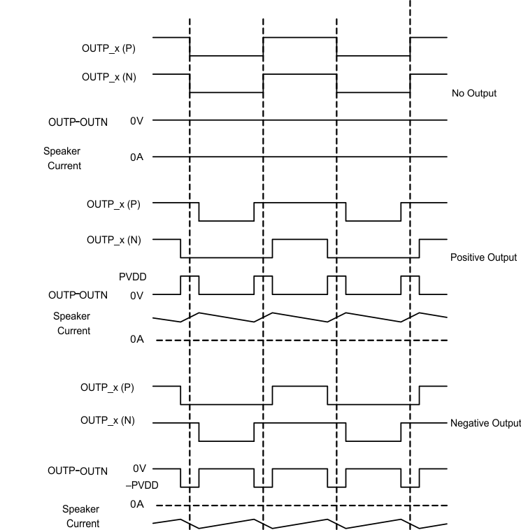 Figure 25. BD Modulation Switching Waveforms
8.4.5 Device Reset
When RESET is asserted low, all power-stage FETs in the four half-bridges are forced into a high-impedance (Hi-Z) state.
In BTL modes, to accommodate bootstrap charging prior to switching start, asserting the reset input low enables weak pulldown of the half-bridge outputs. In the SE mode, the output is forced into a high impedance state when asserting the reset input low. Asserting reset input low removes any fault information to be signaled on the FAULT output, i.e., FAULT is forced high. A rising-edge transition on reset input allows the device to resume operation after an overload fault. To ensure thermal reliability, the rising edge of RESET must occur no sooner than 4 ms after the falling edge of FAULT.
8.4.6 Unused Output Channels
If any output channels are unused, it is recommended to disable switching of unused output nodes to reduce power consumption. Furthermore by disabling unused output channels the cost of unused output LC demodulation filters can be avoided.
Disable a channel by leaving the bootstrap capacitor (BST) unpopulated and connecting the respective input to GND. The unused output pin(s) can be left floating. Please note that the PVDD decoupling capacitors still need to be populated.
Table 6. Unused Output Channels
| Operating Mode | PWM Input | Output Configuration | Unused Channel | INPUT_A | INPUT_B | INPUT_C | INPUT_D | Unpopulated Component(s) |
|---|---|---|---|---|---|---|---|---|
| 000 | 2N | 2 x BTL | AB CD |
GND PWMa |
GND PWMb |
PWMc GND |
PWMd GND |
BST_A & BST_B capacitor BST_C & BST_D capacitor |
| 001 | 1N | |||||||
| 010 | 2N | |||||||
| 101 | 1N | 4 x SE | A | GND | PWMb | PWMc | PWMd | BST_A capacitor |
| B | PWMa | GND | PWMc | PWMd | BST_B capacitor | |||
| C | PWMa | PWMb | GND | PWMd | BST_C capacitor | |||
| D | PWMa | PWMb | PWMc | GND | BST_D capacitor |