ZHCSH21A
October 2017 – February 2018
UCC28780
PRODUCTION DATA.
1
特性
2
应用
3
说明
Device Images
简化原理图
45W、20V GaN-ACF 适配器效率
4
修订历史记录
5
Pin Configuration and Functions
Pin Functions
6
Specifications
6.1
Absolute Maximum Ratings
6.2
ESD Ratings
6.3
Recommended Operating Conditions
6.4
Thermal Information of SOIC
6.5
Thermal Information of WQFN
6.6
Electrical Characteristics
6.7
Typical Characteristics
7
Detailed Description
7.1
Overview
7.2
Functional Block Diagram
7.3
Detailed Pin Description
7.3.1
BUR Pin (Programmable Burst Mode)
7.3.2
FB Pin (Feedback Pin)
7.3.3
VDD Pin (Device Bias Supply)
7.3.4
REF Pin (Internal 5-V Bias)
7.3.5
HVG and SWS Pins
7.3.6
RTZ Pin (Sets Delay for Transition Time to Zero)
7.3.7
RDM Pin (Sets Synthesized Demagnetization Time for ZVS Tuning)
7.3.8
RUN Pin (Driver Enable Pin)
7.3.9
SET Pin
7.4
Device Functional Modes
7.4.1
Adaptive ZVS Control with Auto-Tuning
7.4.2
Dead-Time Optimization
7.4.3
Control Law across Entire Load Range
7.4.4
Adaptive Amplitude Modulation (AAM)
7.4.5
Adaptive Burst Mode (ABM)
7.4.6
Low Power Mode (LPM)
7.4.7
Standby Power Mode (SBP)
7.4.8
Startup Sequence
7.4.9
Survival Mode of VDD
7.4.10
System Fault Protections
7.4.10.1
Brown-In and Brown-Out
7.4.10.2
Output Over-Voltage Protection
7.4.10.3
Over-Temperature Protection
7.4.10.4
Programmable Over-Power Protection
7.4.10.5
Peak Current Limit
7.4.10.6
Output Short-Circuit Protection
7.4.10.7
Over-Current Protection
7.4.10.8
Thermal Shutdown
7.4.11
Pin Open/Short Protections
7.4.11.1
Protections on CS pin Fault
7.4.11.2
Protections on HVG pin Fault
7.4.11.3
Protections on RDM and RTZ pin Faults
8
Application and Implementation
8.1
Application Information
8.2
Typical Application Circuit
8.2.1
Design Requirements
8.2.2
Detailed Design Procedure
8.2.2.1
Input Bulk Capacitance and Minimum Bulk Voltage
8.2.2.2
Transformer Calculations
8.2.2.2.1
Primary-to-Secondary Turns Ratio (NPS)
8.2.2.2.2
Primary Magnetizing Inductance (LM)
8.2.2.2.3
Primary Turns (NP)
8.2.2.2.4
Secondary Turns (NS)
8.2.2.2.5
Turns of Auxiliary Winding (NA)
8.2.2.2.6
Winding and Magnetic Core Materials
8.2.2.3
Clamp Capacitor Calculation
8.2.2.4
Bleed-Resistor Calculation
8.2.2.5
Output Filter Calculation
8.2.2.6
Calculation of ZVS Sensing Network
8.2.2.7
Calculation of Compensation Network
8.2.3
Application Curves
9
Power Supply Recommendations
10
Layout
10.1
Layout Guidelines
10.1.1
General Considerations
10.1.2
RDM and RTZ Pins
10.1.3
SWS Pin
10.1.4
VS Pin
10.1.5
BUR Pin
10.1.6
FB Pin
10.1.7
CS Pin
10.1.8
GND Pin
10.2
Layout Example
11
器件和文档支持
11.1
文档支持
11.1.1
相关文档
11.2
接收文档更新通知
11.3
社区资源
11.4
商标
11.5
静电放电警告
11.6
Glossary
12
机械、封装和可订购信息
6.7
Typical Characteristics
V
VDD
= 15V, R
RDM
= 115 kΩ, R
RTZ
= 140 kΩ, V
SET
= 0 V, and T
J
= T
A
= 25 ⁰C (unless otherwise noted)
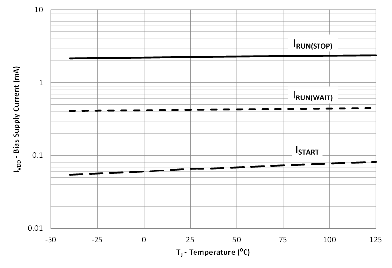
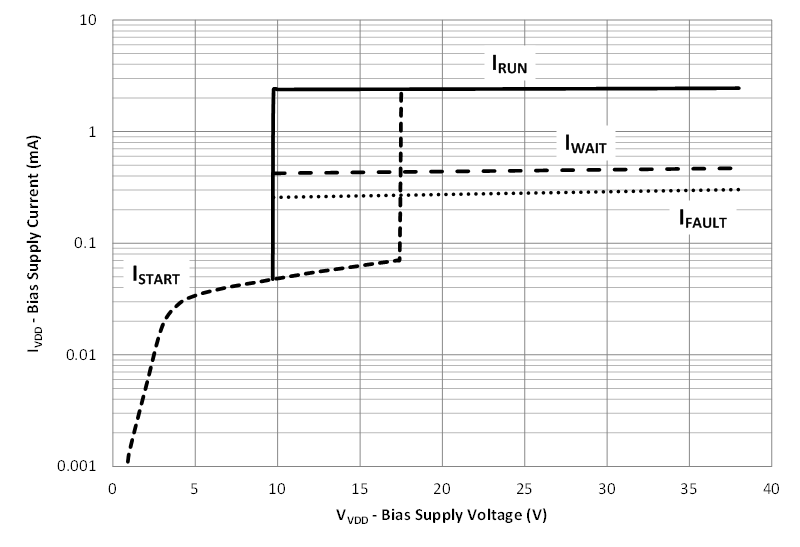
Figure 1.
VDD Bias-Supply Current vs. VDD Bias-Supply Voltage
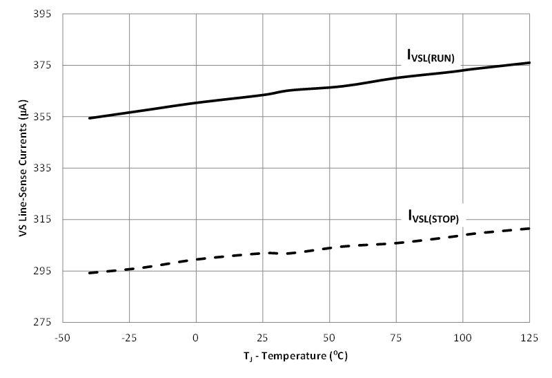
Figure 3.
VS Line-Sense Currents vs. Temperature
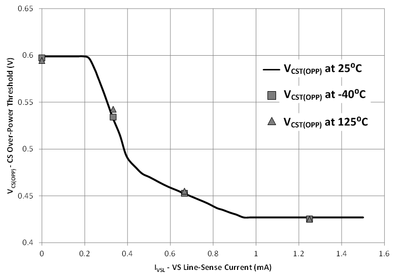
Figure 5.
CS Over-Power Threshold vs. VS Line-Sense Currents
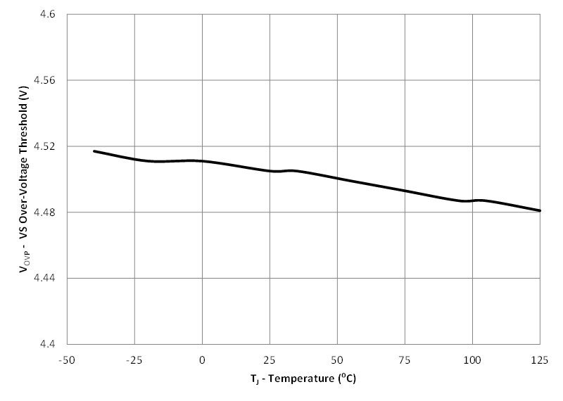
Figure 7.
VS Over-Voltage Threshold vs. Temperature
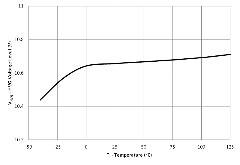
Figure 9.
HVG Voltage vs. Temperature
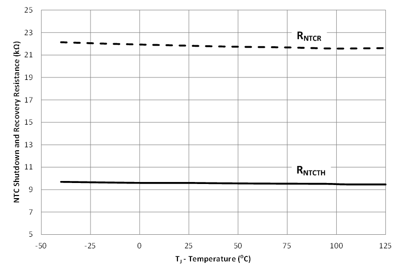
Figure 11.
NTC Thresholds vs. Junction Temperature
Figure 2.
VDD Bias-Supply Current vs. Junction Temperature
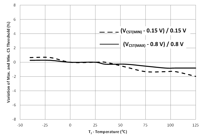
Figure 4.
Percentage Variation of Maximum and Minimum CS Thresholds vs. Temperature
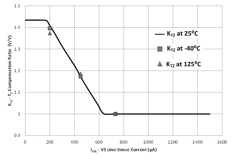
Figure 6.
t
Z
Compensation Ratio (K
TZ
) vs. VS Line-Sense Currents
Figure 8.
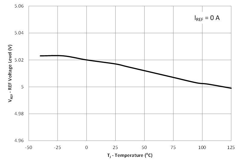
REF Voltage vs. Temperature
Figure 10.
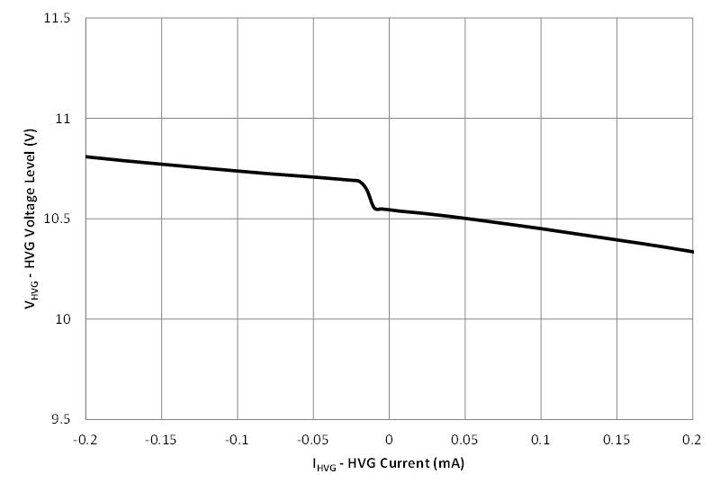
HVG Voltage vs. HVG Current
千亿体育app官网登录(中国)官方网站IOS/安卓通用版/手机APP
|
米乐app下载官网(中国)|ios|Android/通用版APP最新版
|
米乐|米乐·M6(中国大陆)官方网站
|
千亿体育登陆地址
|
华体会体育(中国)HTH·官方网站
|
千赢qy国际_全站最新版千赢qy国际V6.2.14安卓/IOS下载
|
18新利网v1.2.5|中国官方网站
|
bob电竞真人(中国官网)安卓/ios苹果/电脑版【1.97.95版下载】
|
千亿体育app官方下载(中国)官方网站IOS/安卓/手机APP下载安装
|