ZHCSH26E March   2017  – May 2021 CC3120MOD

PRODUCTION DATA  

  1. 特性
  2. 应用
  3. 说明
  4. 功能方框图
  5. Revision History
  6. Device Comparison
    1. 6.1 Related Products
  7. Terminal Configuration and Functions
    1. 7.1 CC3120MOD Pin Diagram
    2. 7.2 Pin Attributes
      1.      11
    3. 7.3 Connections for Unused Pins
  8. Specifications
    1. 8.1  Absolute Maximum Ratings
    2. 8.2  ESD Ratings
    3. 8.3  Recommended Operating Conditions
    4. 8.4  Current Consumption Summary
    5. 8.5  TX Power and IBAT versus TX Power Level Settings
    6. 8.6  Brownout and Blackout Conditions
    7. 8.7  Electrical Characteristics
    8. 8.8  WLAN Receiver Characteristics
    9. 8.9  WLAN Transmitter Characteristics
    10. 8.10 Reset Requirement
    11. 8.11 Thermal Resistance Characteristics for MOB Package
    12. 8.12 Timing and Switching Characteristics
      1. 8.12.1 Power-Up Sequencing
      2. 8.12.2 Power-Down Sequencing
      3. 8.12.3 Device Reset
      4. 8.12.4 Wakeup From HIBERNATE Mode Timing
    13. 8.13 External Interfaces
      1. 8.13.1 SPI Host Interface
      2. 8.13.2 Host UART Interface
        1. 8.13.2.1 5-Wire UART Topology
        2. 8.13.2.2 4-Wire UART Topology
        3. 8.13.2.3 3-Wire UART Topology
      3. 8.13.3 External Flash Interface
  9. Detailed Description
    1. 9.1 Overview
    2. 9.2 Module Features
      1. 9.2.1 WLAN
      2. 9.2.2 Network Stack
        1. 9.2.2.1 Security
      3. 9.2.3 Host Interface and Driver
      4. 9.2.4 System
    3. 9.3 Power-Management Subsystem
      1. 9.3.1 VBAT Wide-Voltage Connection
    4. 9.4 Low-Power Operating Modes
      1. 9.4.1 Low-Power Deep Sleep
      2. 9.4.2 Hibernate
      3. 9.4.3 Shutdown
    5. 9.5 Restoring Factory Default Configuration
    6. 9.6 Device Certification and Qualification
      1. 9.6.1 FCC Certification and Statement
      2. 9.6.2 Industry Canada (IC) Certification and Statement
      3. 9.6.3 ETSI/CE Certification
      4. 9.6.4 Japan MIC Certification
      5. 9.6.5 SRRC Certification and Statement
    7. 9.7 Module Markings
    8. 9.8 End Product Labeling
    9. 9.9 Manual Information to the End User
  10. 10Applications, Implementation, and Layout
    1. 10.1 Application Information
      1. 10.1.1 Typical Application
      2. 10.1.2 Power Supply Decoupling and Bulk Capacitors
      3. 10.1.3 Reset
      4. 10.1.4 Unused Pins
    2. 10.2 PCB Layout Guidelines
      1. 10.2.1 General Layout Recommendations
      2. 10.2.2 RF Layout Recommendations
      3. 10.2.3 Antenna Placement and Routing
      4. 10.2.4 Transmission Line Considerations
  11. 11Environmental Requirements and Specifications
    1. 11.1 Temperature
      1. 11.1.1 PCB Bending
    2. 11.2 Handling Environment
      1. 11.2.1 Terminals
      2. 11.2.2 Falling
    3. 11.3 Storage Condition
      1. 11.3.1 Moisture Barrier Bag Before Opened
      2. 11.3.2 Moisture Barrier Bag Open
    4. 11.4 Baking Conditions
    5. 11.5 Soldering and Reflow Condition
  12. 12Device and Documentation Support
    1. 12.1 Device Nomenclature
    2. 12.2 Development Tools and Software
    3. 12.3 Firmware Updates
    4. 12.4 Documentation Support
    5. 12.5 Trademarks
    6. 12.6 Electrostatic Discharge Caution
    7. 12.7 术语表
  13. 13Mechanical, Packaging, and Orderable Information
    1. 13.1 Mechanical, Land, and Solder Paste Drawings
    2. 13.2 Package Option Addendum
      1. 13.2.1 Packaging Information
    3. 13.3 Tape and Reel Information
      1. 13.3.1 Tape and Reel Specification

RF Layout Recommendations

The RF section of this wireless device gets top priority in terms of layout. It is very important for the RF section to be laid out correctly to ensure optimum performance from the device. A poor layout can cause low-output power, EVM degradation, sensitivity degradation, and mask violations.

Figure 10-2 shows the RF placement and routing of the CC3120MOD module.
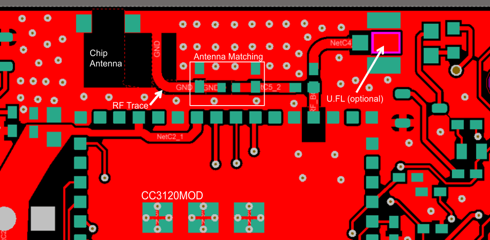
GUID-7F5BDC21-B1AC-424D-BA5C-6D15DC53F7AB-low.gif Figure 10-2 RF Section Layout

For optimal RF performance, ensure the copper cut out on the top layer under the RF-BG pin, (pin 31), is as shown in Figure 10-3.
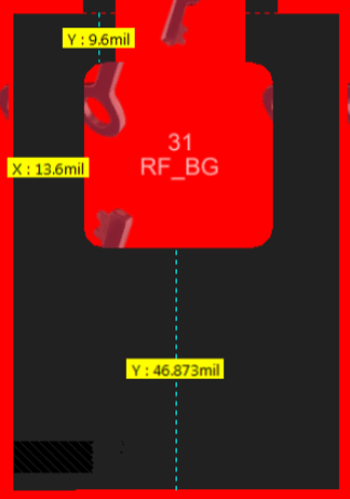
GUID-447D81F8-C9BC-476C-A558-D8134ACC9339-low.gif Figure 10-3 Top Layer Copper Pull Back on RF Pads