ZHCSH26E March   2017  – May 2021 CC3120MOD

PRODUCTION DATA  

  1. 特性
  2. 应用
  3. 说明
  4. 功能方框图
  5. Revision History
  6. Device Comparison
    1. 6.1 Related Products
  7. Terminal Configuration and Functions
    1. 7.1 CC3120MOD Pin Diagram
    2. 7.2 Pin Attributes
      1.      11
    3. 7.3 Connections for Unused Pins
  8. Specifications
    1. 8.1  Absolute Maximum Ratings
    2. 8.2  ESD Ratings
    3. 8.3  Recommended Operating Conditions
    4. 8.4  Current Consumption Summary
    5. 8.5  TX Power and IBAT versus TX Power Level Settings
    6. 8.6  Brownout and Blackout Conditions
    7. 8.7  Electrical Characteristics
    8. 8.8  WLAN Receiver Characteristics
    9. 8.9  WLAN Transmitter Characteristics
    10. 8.10 Reset Requirement
    11. 8.11 Thermal Resistance Characteristics for MOB Package
    12. 8.12 Timing and Switching Characteristics
      1. 8.12.1 Power-Up Sequencing
      2. 8.12.2 Power-Down Sequencing
      3. 8.12.3 Device Reset
      4. 8.12.4 Wakeup From HIBERNATE Mode Timing
    13. 8.13 External Interfaces
      1. 8.13.1 SPI Host Interface
      2. 8.13.2 Host UART Interface
        1. 8.13.2.1 5-Wire UART Topology
        2. 8.13.2.2 4-Wire UART Topology
        3. 8.13.2.3 3-Wire UART Topology
      3. 8.13.3 External Flash Interface
  9. Detailed Description
    1. 9.1 Overview
    2. 9.2 Module Features
      1. 9.2.1 WLAN
      2. 9.2.2 Network Stack
        1. 9.2.2.1 Security
      3. 9.2.3 Host Interface and Driver
      4. 9.2.4 System
    3. 9.3 Power-Management Subsystem
      1. 9.3.1 VBAT Wide-Voltage Connection
    4. 9.4 Low-Power Operating Modes
      1. 9.4.1 Low-Power Deep Sleep
      2. 9.4.2 Hibernate
      3. 9.4.3 Shutdown
    5. 9.5 Restoring Factory Default Configuration
    6. 9.6 Device Certification and Qualification
      1. 9.6.1 FCC Certification and Statement
      2. 9.6.2 Industry Canada (IC) Certification and Statement
      3. 9.6.3 ETSI/CE Certification
      4. 9.6.4 Japan MIC Certification
      5. 9.6.5 SRRC Certification and Statement
    7. 9.7 Module Markings
    8. 9.8 End Product Labeling
    9. 9.9 Manual Information to the End User
  10. 10Applications, Implementation, and Layout
    1. 10.1 Application Information
      1. 10.1.1 Typical Application
      2. 10.1.2 Power Supply Decoupling and Bulk Capacitors
      3. 10.1.3 Reset
      4. 10.1.4 Unused Pins
    2. 10.2 PCB Layout Guidelines
      1. 10.2.1 General Layout Recommendations
      2. 10.2.2 RF Layout Recommendations
      3. 10.2.3 Antenna Placement and Routing
      4. 10.2.4 Transmission Line Considerations
  11. 11Environmental Requirements and Specifications
    1. 11.1 Temperature
      1. 11.1.1 PCB Bending
    2. 11.2 Handling Environment
      1. 11.2.1 Terminals
      2. 11.2.2 Falling
    3. 11.3 Storage Condition
      1. 11.3.1 Moisture Barrier Bag Before Opened
      2. 11.3.2 Moisture Barrier Bag Open
    4. 11.4 Baking Conditions
    5. 11.5 Soldering and Reflow Condition
  12. 12Device and Documentation Support
    1. 12.1 Device Nomenclature
    2. 12.2 Development Tools and Software
    3. 12.3 Firmware Updates
    4. 12.4 Documentation Support
    5. 12.5 Trademarks
    6. 12.6 Electrostatic Discharge Caution
    7. 12.7 术语表
  13. 13Mechanical, Packaging, and Orderable Information
    1. 13.1 Mechanical, Land, and Solder Paste Drawings
    2. 13.2 Package Option Addendum
      1. 13.2.1 Packaging Information
    3. 13.3 Tape and Reel Information
      1. 13.3.1 Tape and Reel Specification

Typical Application

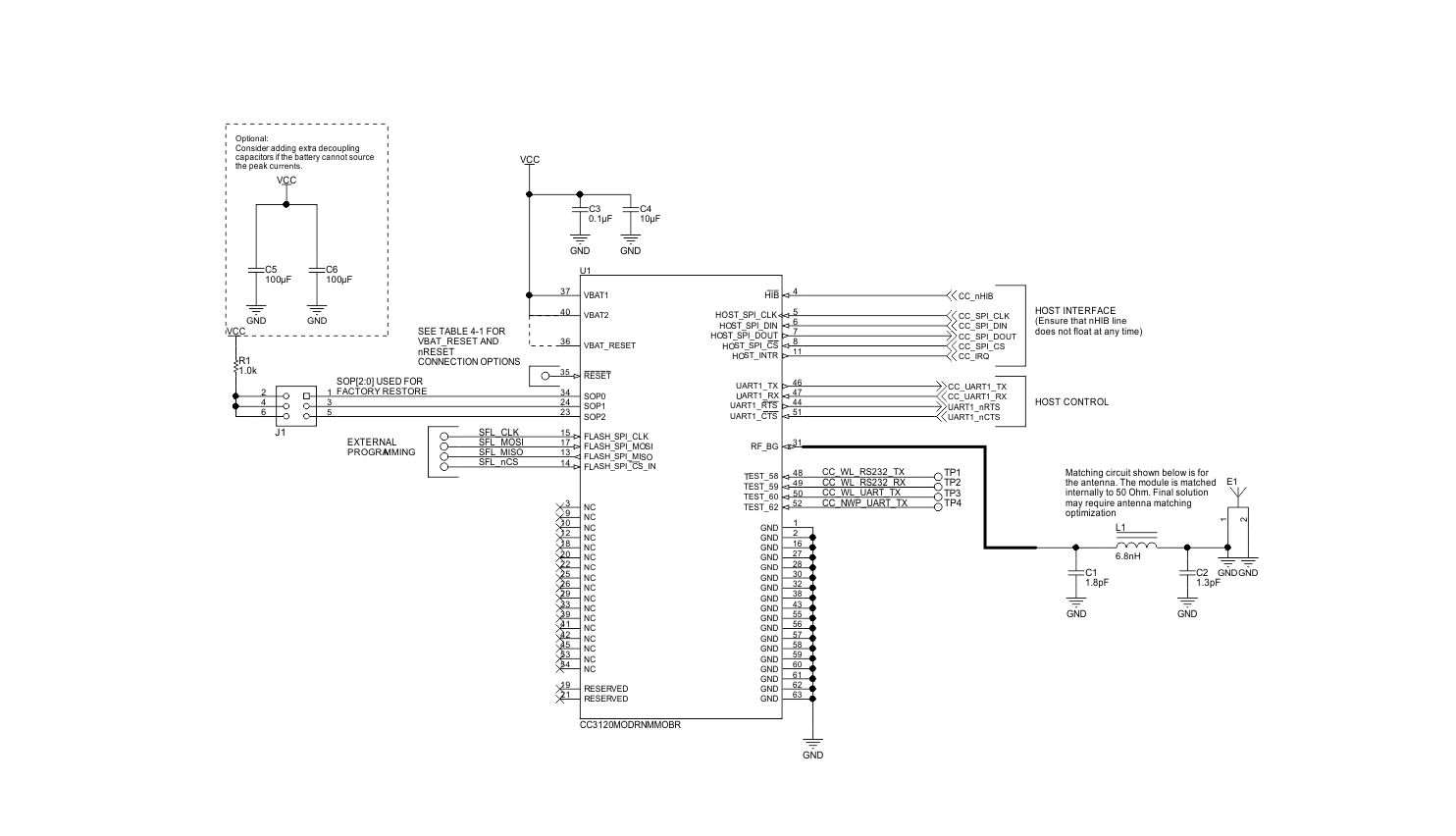
Figure 10-1 shows the typical application schematic using the CC3120MOD module. For a full operation reference design, see the BoosterPack that uses the CC3120MOD module.
GUID-D701D4E8-FDC8-4F7A-8395-99C15C00346D-low.gif
This is the reference schematic and not an actual board design. For the board files and BOM, refer to the CC3120MODBOOST in the CC3120MOD Tools Folder.
Figure 10-1 CC3120MOD Module Reference Schematic

Table 10-1 lists the bill of materials for a typical application using the CC3120MOD module shown in Figure 10-1.

Table 10-1 Bill of Materials
QUANTITY DESIGNATOR VALUE MANUFACTURER PART NUMBER DESCRIPTION
1 C1 1.8 pF MuRata GCM1555C1H1R8BA16 CAP, CERM, 1.8 pF, 50 V,
±0.1 pF, C0G/NP0, 0402
1 C2 1.3 pF MuRata GCM1555C1H1R3BA16 CAP, CERM, 1.3 pF, 50 V, ±5%, C0G/NP0, 0402
1 C3 0.1 µF MuRata GRM155R60J104KA01D CAP, CERM, 0.1 µF, 6.3 V, ±10%, X5R, 0402
1 C4 10 µF MuRata GRM21BR61A106KE19L CAP, CERM, 10 µF, 10 V, ±10%, X5R, 0805
2 C5, C6 100 µF MuRata GRM31CR60J107ME39L CAP, CERM, 100 µF, 6.3 V, ±20%, X5R, 1206
1 E1 2.45-GHz Ant Taiyo Yuden AH316M245001-T ANT BLUETOOTH W-LAN ZIGBEE WIMAX, SMD
1 L1 6.8 nH MuRata LQP15MN6N8B02 6.8 nH Unshielded Thin Film Inductor 130 mA 900 mΩ Max 0402
1 R1 1.0 k Vishay-Dale CRCW04021K00JNED RES, 1.0 k, 5%, 0.063 W, 0402
1 U1 CC3120MOD Texas Instruments CC3120MODRNMMOBR SimpleLink Certified Wi-Fi Network Processor Internet-of-Things Module Solution for MCU Applications, MOB0063A (SIP MODULE-63)