ZHCSH63B October   2017  – January 2020 TLC6C5816-Q1

PRODUCTION DATA.  

  1. 特性
  2. 应用
  3. 说明
    1.     典型应用原理图
  4. 修订历史记录
  5. Pin Configuration and Functions
    1.     Pin Functions
  6. Specifications
    1. 6.1 Absolute Maximum Ratings
    2. 6.2 ESD Ratings
    3. 6.3 Recommended Operating Conditions
    4. 6.4 Thermal Information
    5. 6.5 Electrical Characteristics
    6. 6.6 Timing Requirements
    7. 6.7 Switching Characteristics
    8. 6.8 Typical Characteristics
  7. Detailed Description
    1. 7.1 Overview
    2. 7.2 Functional Block Diagram
    3. 7.3 Feature Description
      1. 7.3.1 Device Enable (EN)
      2. 7.3.2 Gated Output (Gx)
      3. 7.3.3 Register Clear (CLR)
      4. 7.3.4 Open-Drain Outputs and Flexible Diagnostics Channel
        1. 7.3.4.1 Configurable Outputs
        2. 7.3.4.2 LED-Open Diagnostics
        3. 7.3.4.3 LED-Short Diagnostics
      5. 7.3.5 Thermal Shutdown
      6. 7.3.6 Command Error
      7. 7.3.7 Serial Communication Error
      8. 7.3.8 Error Feedback
      9. 7.3.9 Interface
        1. 7.3.9.1 Register Write
        2. 7.3.9.2 Register Read
        3. 7.3.9.3 Shift-Register Communication-Fault Detection
        4. 7.3.9.4 Clear Register
        5. 7.3.9.5 Register Clock
    4. 7.4 Device Functional Modes
      1. 7.4.1 Normal Operation
      2. 7.4.2 POR Reset
      3. 7.4.3 Standby Mode
    5. 7.5 Register Maps
    6. 7.6 Interface Registers
      1. 7.6.1 Configuration Register (Offset = 0h) [reset = 0h]
        1. Table 5. Configuration Register Field Descriptions
      2. 7.6.2 Fault Readback Register (Offset = 1h) [reset = 0h]
        1. Table 6. Fault Readback Register Field Descriptions
  8. Application and Implementation
    1. 8.1 Application Information
    2. 8.2 Typical Application
      1. 8.2.1 Design Requirements
      2. 8.2.2 Detailed Design Procedure
      3. 8.2.3 Application Curves
  9. Power Supply Recommendations
  10. 10Layout
    1. 10.1 Layout Guidelines
    2. 10.2 Layout Example
  11. 11器件和文档支持
    1. 11.1 接收文档更新通知
    2. 11.2 社区资源
    3. 11.3 商标
    4. 11.4 静电放电警告
    5. 11.5 Glossary
  12. 12机械、封装和可订购信息

Typical Characteristics

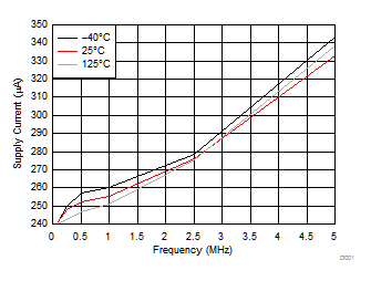
TLC6C5816-Q1 D001_SLASEJ5.gif
VCC = 5 V
Figure 3. Supply Current vs CLK Frequency
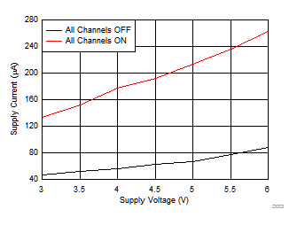
TLC6C5816-Q1 D003_SLASEJ5.gif
Figure 5. Supply Current vs Supply Voltage
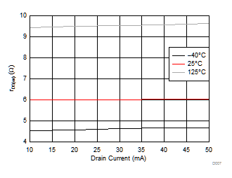
TLC6C5816-Q1 D007_SLASEJ5.gif
VCC = 5 V Single channel ON
Figure 7. rDS(on)vs Ambient Temperature
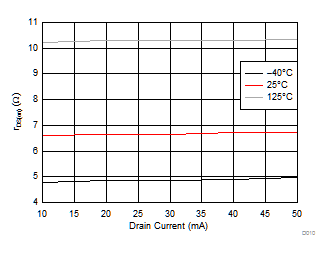
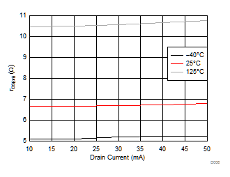
TLC6C5816-Q1 D010_SLASEJ5.gif
VCC = 5 V All channels ON
Figure 9. rDS(on) vs Drain Current
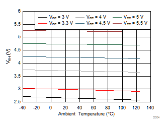
TLC6C5816-Q1 D004_SLASEJ5.gif
Figure 11. SER OUT High Voltage vs Temperature (°C)
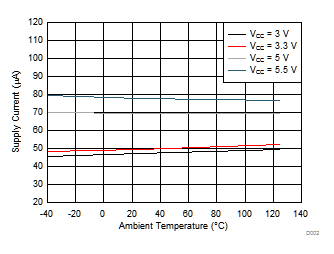
TLC6C5816-Q1 D002_SLASEJ5.gif
Figure 4. Supply Current vs Ambient Temperature
TLC6C5816-Q1 D006_SLASEJ5.gif
VCC = 3.3 V Single channel ON
Figure 6. rDS(on) vs Ambient Temperature
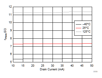
TLC6C5816-Q1 D009_SLASEJ5.gif
VCC = 3.3 V All channels ON
Figure 8. rDS(on)vs Drain Current
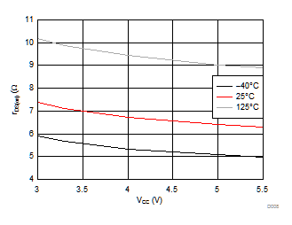
TLC6C5816-Q1 D008_SLASEJ5.gif
Figure 10. rDS(on) vs Supply Voltage
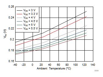
TLC6C5816-Q1 D005_SLASEJ5.gif
Figure 12. SER OUT Low Voltage vs Temperature (°C)