ZHCSH63B October   2017  – January 2020 TLC6C5816-Q1

PRODUCTION DATA.  

  1. 特性
  2. 应用
  3. 说明
    1.     典型应用原理图
  4. 修订历史记录
  5. Pin Configuration and Functions
    1.     Pin Functions
  6. Specifications
    1. 6.1 Absolute Maximum Ratings
    2. 6.2 ESD Ratings
    3. 6.3 Recommended Operating Conditions
    4. 6.4 Thermal Information
    5. 6.5 Electrical Characteristics
    6. 6.6 Timing Requirements
    7. 6.7 Switching Characteristics
    8. 6.8 Typical Characteristics
  7. Detailed Description
    1. 7.1 Overview
    2. 7.2 Functional Block Diagram
    3. 7.3 Feature Description
      1. 7.3.1 Device Enable (EN)
      2. 7.3.2 Gated Output (Gx)
      3. 7.3.3 Register Clear (CLR)
      4. 7.3.4 Open-Drain Outputs and Flexible Diagnostics Channel
        1. 7.3.4.1 Configurable Outputs
        2. 7.3.4.2 LED-Open Diagnostics
        3. 7.3.4.3 LED-Short Diagnostics
      5. 7.3.5 Thermal Shutdown
      6. 7.3.6 Command Error
      7. 7.3.7 Serial Communication Error
      8. 7.3.8 Error Feedback
      9. 7.3.9 Interface
        1. 7.3.9.1 Register Write
        2. 7.3.9.2 Register Read
        3. 7.3.9.3 Shift-Register Communication-Fault Detection
        4. 7.3.9.4 Clear Register
        5. 7.3.9.5 Register Clock
    4. 7.4 Device Functional Modes
      1. 7.4.1 Normal Operation
      2. 7.4.2 POR Reset
      3. 7.4.3 Standby Mode
    5. 7.5 Register Maps
    6. 7.6 Interface Registers
      1. 7.6.1 Configuration Register (Offset = 0h) [reset = 0h]
        1. Table 5. Configuration Register Field Descriptions
      2. 7.6.2 Fault Readback Register (Offset = 1h) [reset = 0h]
        1. Table 6. Fault Readback Register Field Descriptions
  8. Application and Implementation
    1. 8.1 Application Information
    2. 8.2 Typical Application
      1. 8.2.1 Design Requirements
      2. 8.2.2 Detailed Design Procedure
      3. 8.2.3 Application Curves
  9. Power Supply Recommendations
  10. 10Layout
    1. 10.1 Layout Guidelines
    2. 10.2 Layout Example
  11. 11器件和文档支持
    1. 11.1 接收文档更新通知
    2. 11.2 社区资源
    3. 11.3 商标
    4. 11.4 静电放电警告
    5. 11.5 Glossary
  12. 12机械、封装和可订购信息

Configurable Outputs

The 16 channels are divided into eight pairs of outputs like DRAIN0, DRAIN1/DIAG0 as shown in Figure 13. By default, both outputs of this pair are open-drain outputs. Each of the pair is independent from the other.
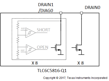
TLC6C5816-Q1 Output-SLASEJ5.gifFigure 13. Open-Drain Output and Flexible Diagnostics

By setting its bit in the configuration register to HIGH, the DRAIN1/DIAG0 output can be configured as diagnostics channel DIAG0 for DRAIN0.

By setting the configuration register to LOW, DRAIN1/DIAG0 can be configured as the independent open-drain output DRAIN1.

If DRAIN1/DIGA0 is configured as a diagnostics channel, when DRAIN0 is on, the DRAIN1/DIAG0 diagnostics path monitors the voltage. When DRAIN0 is off, DRAIN1/DIAG0 is in the high-impedance state to avoid any leakage current.
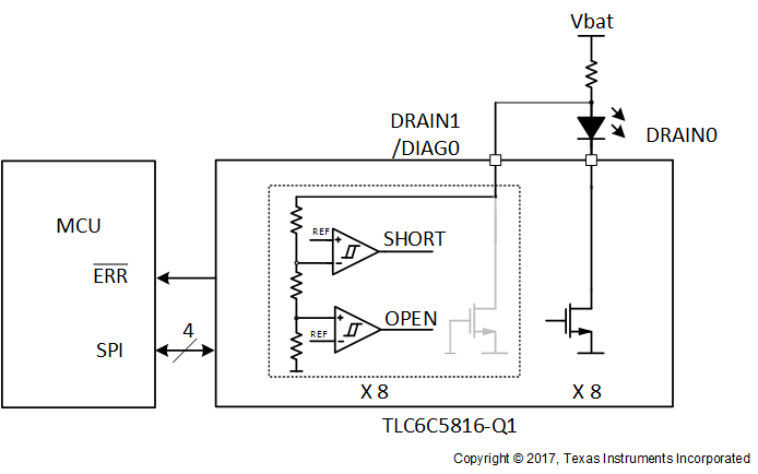
TLC6C5816-Q1 Diag-SLASEJ5.gifFigure 14. Diagnostics Configuration of Output Driver Pair