ZHCSHA6E May   2009  – January 2018 ADS1013 , ADS1014 , ADS1015

PRODUCTION DATA.  

  1. 特性
  2. 应用
  3. 说明
    1.     Device Images
      1.      简化的方框图
  4. Revision History
  5. Device Comparison Table
  6. Pin Configuration and Functions
    1.     Pin Functions
  7. Specifications
    1. 7.1 Absolute Maximum Ratings
    2. 7.2 ESD Ratings
    3. 7.3 Recommended Operating Conditions
    4. 7.4 Thermal Information
    5. 7.5 Electrical Characteristics
    6. 7.6 Timing Requirements: I2C
    7. 7.7 Typical Characteristics
  8. Detailed Description
    1. 8.1 Overview
    2. 8.2 Functional Block Diagrams
    3. 8.3 Feature Description
      1. 8.3.1 Multiplexer
      2. 8.3.2 Analog Inputs
      3. 8.3.3 Full-Scale Range (FSR) and LSB Size
      4. 8.3.4 Voltage Reference
      5. 8.3.5 Oscillator
      6. 8.3.6 Output Data Rate and Conversion Time
      7. 8.3.7 Digital Comparator (ADS1014 and ADS1015 Only)
      8. 8.3.8 Conversion Ready Pin (ADS1014 and ADS1015 Only)
      9. 8.3.9 SMbus Alert Response
    4. 8.4 Device Functional Modes
      1. 8.4.1 Reset and Power-Up
      2. 8.4.2 Operating Modes
        1. 8.4.2.1 Single-Shot Mode
        2. 8.4.2.2 Continuous-Conversion Mode
      3. 8.4.3 Duty Cycling For Low Power
    5. 8.5 Programming
      1. 8.5.1 I2C Interface
        1. 8.5.1.1 I2C Address Selection
        2. 8.5.1.2 I2C General Call
        3. 8.5.1.3 I2C Speed Modes
      2. 8.5.2 Slave Mode Operations
        1. 8.5.2.1 Receive Mode
        2. 8.5.2.2 Transmit Mode
      3. 8.5.3 Writing To and Reading From the Registers
      4. 8.5.4 Data Format
    6. 8.6 Register Map
      1. 8.6.1 Address Pointer Register (address = N/A) [reset = N/A]
        1. Table 4. Address Pointer Register Field Descriptions
      2. 8.6.2 Conversion Register (P[1:0] = 0h) [reset = 0000h]
        1. Table 5. Conversion Register Field Descriptions
      3. 8.6.3 Config Register (P[1:0] = 1h) [reset = 8583h]
        1. Table 6. Config Register Field Descriptions
      4. 8.6.4 Lo_thresh (P[1:0] = 2h) [reset = 8000h] and Hi_thresh (P[1:0] = 3h) [reset = 7FFFh] Registers
        1. Table 7. Lo_thresh and Hi_thresh Register Field Descriptions
  9. Application and Implementation
    1. 9.1 Application Information
      1. 9.1.1 Basic Connections
      2. 9.1.2 Single-Ended Inputs
      3. 9.1.3 Input Protection
      4. 9.1.4 Unused Inputs and Outputs
      5. 9.1.5 Analog Input Filtering
      6. 9.1.6 Connecting Multiple Devices
      7. 9.1.7 Quickstart Guide
    2. 9.2 Typical Application
      1. 9.2.1 Design Requirements
      2. 9.2.2 Detailed Design Procedure
        1. 9.2.2.1 Shunt Resistor Considerations
        2. 9.2.2.2 Operational Amplifier Considerations
        3. 9.2.2.3 ADC Input Common-Mode Considerations
        4. 9.2.2.4 Resistor (R1, R2, R3, R4) Considerations
        5. 9.2.2.5 Noise and Input Impedance Considerations
        6. 9.2.2.6 First-order RC Filter Considerations
        7. 9.2.2.7 Circuit Implementation
        8. 9.2.2.8 Results Summary
      3. 9.2.3 Application Curves
  10. 10Power Supply Recommendations
    1. 10.1 Power-Supply Sequencing
    2. 10.2 Power-Supply Decoupling
  11. 11Layout
    1. 11.1 Layout Guidelines
    2. 11.2 Layout Example
  12. 12器件和文档支持
    1. 12.1 Documentation Support
      1. 12.1.1 Related Documentation
    2. 12.2 相关链接
    3. 12.3 Receiving Notification of Documentation Updates
    4. 12.4 Community Resources
    5. 12.5 商标
    6. 12.6 静电放电警告
    7. 12.7 Glossary
  13. 13机械、封装和可订购信息

Writing To and Reading From the Registers

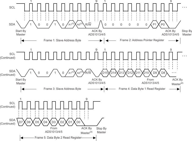
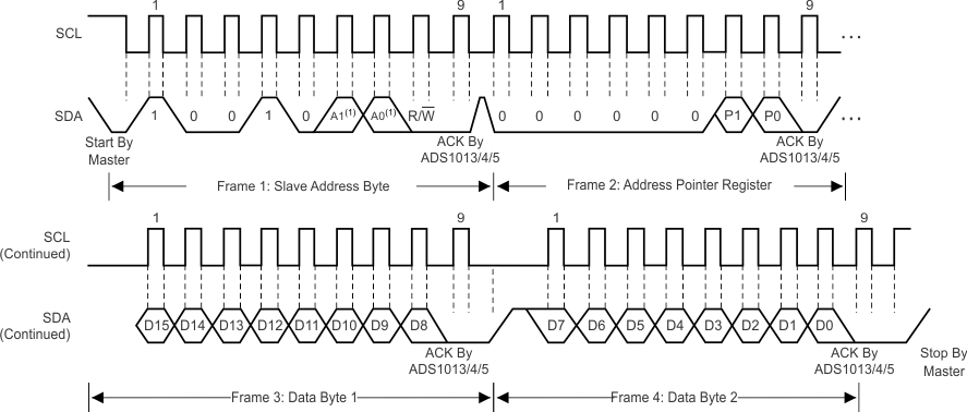
To access a specific register from the ADS101x, the master must first write an appropriate value to register address pointer bits P[1:0] in the Address Pointer register. The Address Pointer register is written to directly after the slave address byte, low R/W bit, and a successful slave acknowledgment. After the Address Pointer register is written, the slave acknowledges, and the master issues a STOP or a repeated START condition.

When reading from the ADS101x, the previous value written to bits P[1:0] determines the register that is read. To change which register is read, a new value must be written to P[1:0]. To write a new value to P[1:0], the master issues a slave address byte with the R/W bit low, followed by the Address Pointer register byte. No additional data has to be transmitted, and a STOP condition can be issued by the master. The master can now issue a START condition and send the slave address byte with the R/W bit high to begin the read. Figure 22 details this sequence. If repeated reads from the same register are desired, there is no need to continually send the Address Pointer register, because the ADS101x store the value of P[1:0] until it is modified by a write operation. However, for every write operation, the Address Pointer register must be written with the appropriate values.
ADS1013 ADS1014 ADS1015 ai_tim_2wire_rd_bas473.gif
The values of A0 and A1 are determined by the ADDR pin.
Master can leave SDA high to terminate a single-byte read operation.
Master can leave SDA high to terminate a two-byte read operation.
Figure 15. Timing Diagram for Reading From ADS101x
ADS1013 ADS1014 ADS1015 ai_tim_2wire_wr_bas473.gif
The values of A0 and A1 are determined by the ADDR pin.
Figure 16. Timing Diagram for Writing to ADS101x
ADS1013 ADS1014 ADS1015 ai_tim_smbus_bas473.gif
The values of A0 and A1 are determined by the ADDR pin.
Figure 17. Timing Diagram for SMBus Alert Response