ZHCSHA6E May   2009  – January 2018 ADS1013 , ADS1014 , ADS1015

PRODUCTION DATA.  

  1. 特性
  2. 应用
  3. 说明
    1.     Device Images
      1.      简化的方框图
  4. Revision History
  5. Device Comparison Table
  6. Pin Configuration and Functions
    1.     Pin Functions
  7. Specifications
    1. 7.1 Absolute Maximum Ratings
    2. 7.2 ESD Ratings
    3. 7.3 Recommended Operating Conditions
    4. 7.4 Thermal Information
    5. 7.5 Electrical Characteristics
    6. 7.6 Timing Requirements: I2C
    7. 7.7 Typical Characteristics
  8. Detailed Description
    1. 8.1 Overview
    2. 8.2 Functional Block Diagrams
    3. 8.3 Feature Description
      1. 8.3.1 Multiplexer
      2. 8.3.2 Analog Inputs
      3. 8.3.3 Full-Scale Range (FSR) and LSB Size
      4. 8.3.4 Voltage Reference
      5. 8.3.5 Oscillator
      6. 8.3.6 Output Data Rate and Conversion Time
      7. 8.3.7 Digital Comparator (ADS1014 and ADS1015 Only)
      8. 8.3.8 Conversion Ready Pin (ADS1014 and ADS1015 Only)
      9. 8.3.9 SMbus Alert Response
    4. 8.4 Device Functional Modes
      1. 8.4.1 Reset and Power-Up
      2. 8.4.2 Operating Modes
        1. 8.4.2.1 Single-Shot Mode
        2. 8.4.2.2 Continuous-Conversion Mode
      3. 8.4.3 Duty Cycling For Low Power
    5. 8.5 Programming
      1. 8.5.1 I2C Interface
        1. 8.5.1.1 I2C Address Selection
        2. 8.5.1.2 I2C General Call
        3. 8.5.1.3 I2C Speed Modes
      2. 8.5.2 Slave Mode Operations
        1. 8.5.2.1 Receive Mode
        2. 8.5.2.2 Transmit Mode
      3. 8.5.3 Writing To and Reading From the Registers
      4. 8.5.4 Data Format
    6. 8.6 Register Map
      1. 8.6.1 Address Pointer Register (address = N/A) [reset = N/A]
        1. Table 4. Address Pointer Register Field Descriptions
      2. 8.6.2 Conversion Register (P[1:0] = 0h) [reset = 0000h]
        1. Table 5. Conversion Register Field Descriptions
      3. 8.6.3 Config Register (P[1:0] = 1h) [reset = 8583h]
        1. Table 6. Config Register Field Descriptions
      4. 8.6.4 Lo_thresh (P[1:0] = 2h) [reset = 8000h] and Hi_thresh (P[1:0] = 3h) [reset = 7FFFh] Registers
        1. Table 7. Lo_thresh and Hi_thresh Register Field Descriptions
  9. Application and Implementation
    1. 9.1 Application Information
      1. 9.1.1 Basic Connections
      2. 9.1.2 Single-Ended Inputs
      3. 9.1.3 Input Protection
      4. 9.1.4 Unused Inputs and Outputs
      5. 9.1.5 Analog Input Filtering
      6. 9.1.6 Connecting Multiple Devices
      7. 9.1.7 Quickstart Guide
    2. 9.2 Typical Application
      1. 9.2.1 Design Requirements
      2. 9.2.2 Detailed Design Procedure
        1. 9.2.2.1 Shunt Resistor Considerations
        2. 9.2.2.2 Operational Amplifier Considerations
        3. 9.2.2.3 ADC Input Common-Mode Considerations
        4. 9.2.2.4 Resistor (R1, R2, R3, R4) Considerations
        5. 9.2.2.5 Noise and Input Impedance Considerations
        6. 9.2.2.6 First-order RC Filter Considerations
        7. 9.2.2.7 Circuit Implementation
        8. 9.2.2.8 Results Summary
      3. 9.2.3 Application Curves
  10. 10Power Supply Recommendations
    1. 10.1 Power-Supply Sequencing
    2. 10.2 Power-Supply Decoupling
  11. 11Layout
    1. 11.1 Layout Guidelines
    2. 11.2 Layout Example
  12. 12器件和文档支持
    1. 12.1 Documentation Support
      1. 12.1.1 Related Documentation
    2. 12.2 相关链接
    3. 12.3 Receiving Notification of Documentation Updates
    4. 12.4 Community Resources
    5. 12.5 商标
    6. 12.6 静电放电警告
    7. 12.7 Glossary
  13. 13机械、封装和可订购信息

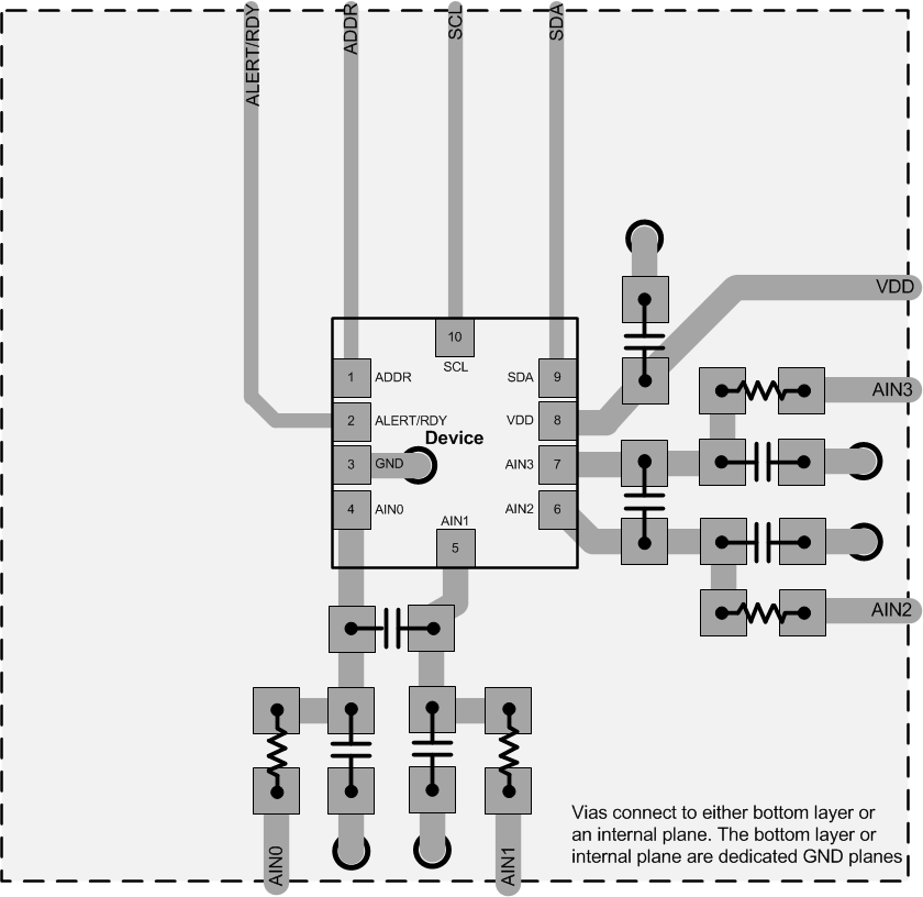
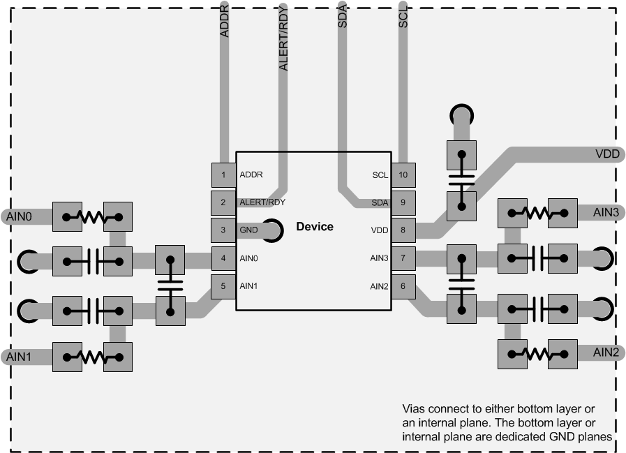
Layout Example

ADS1013 ADS1014 ADS1015 layoutrug_sbas444.gifFigure 34. ADS1015 X2QFN Package
ADS1013 ADS1014 ADS1015 layoutdgs_sbas444.gifFigure 35. ADS1015 VSSOP Package