ZHCSHD5A January   2018  – October 2018 ADS112U04

PRODUCTION DATA.  

  1. 特性
  2. 应用
  3. 说明
    1.     Device Images
      1.      K 型热电偶测量
  4. 修订历史记录
  5. Pin Configuration and Functions
    1.     Pin Functions
  6. Specifications
    1. 6.1 Absolute Maximum Ratings
    2. 6.2 ESD Ratings
    3. 6.3 Recommended Operating Conditions
    4. 6.4 Thermal Information
    5. 6.5 Electrical Characteristics
    6. 6.6 UART Timing Requirements
    7. 6.7 UART Switching Characteristics
    8. 6.8 Typical Characteristics
  7. Parameter Measurement Information
    1. 7.1 Noise Performance
  8. Detailed Description
    1. 8.1 Overview
    2. 8.2 Functional Block Diagram
    3. 8.3 Feature Description
      1. 8.3.1  Multiplexer
      2. 8.3.2  Low-Noise Programmable Gain Stage
        1. 8.3.2.1 PGA Input Voltage Requirements
        2. 8.3.2.2 Bypassing the PGA
      3. 8.3.3  Voltage Reference
      4. 8.3.4  Modulator and Internal Oscillator
      5. 8.3.5  Digital Filter
      6. 8.3.6  Conversion Times
      7. 8.3.7  Excitation Current Sources
      8. 8.3.8  Sensor Detection
      9. 8.3.9  System Monitor
      10. 8.3.10 Temperature Sensor
        1. 8.3.10.1 Converting From Temperature to Digital Codes
          1. 8.3.10.1.1 For Positive Temperatures (For Example, 50°C):
          2. 8.3.10.1.2 For Negative Temperatures (For Example, –25°C):
        2. 8.3.10.2 Converting From Digital Codes to Temperature
      11. 8.3.11 Offset Calibration
      12. 8.3.12 Conversion Data Counter
      13. 8.3.13 Data Integrity
      14. 8.3.14 General-Purpose Digital Inputs/Outputs
    4. 8.4 Device Functional Modes
      1. 8.4.1 Power-Up and Reset
        1. 8.4.1.1 Power-On Reset
        2. 8.4.1.2 RESET Pin
        3. 8.4.1.3 Reset by Command
      2. 8.4.2 Conversion Modes
        1. 8.4.2.1 Single-Shot Conversion Mode
        2. 8.4.2.2 Continuous Conversion Mode
      3. 8.4.3 Operating Modes
        1. 8.4.3.1 Normal Mode
        2. 8.4.3.2 Turbo Mode
        3. 8.4.3.3 Power-Down Mode
    5. 8.5 Programming
      1. 8.5.1 UART Interface
        1. 8.5.1.1 Receive (RX)
        2. 8.5.1.2 Transmit (TX)
        3. 8.5.1.3 Data Ready (DRDY)
        4. 8.5.1.4 Protocol
        5. 8.5.1.5 Timeout
      2. 8.5.2 Data Format
      3. 8.5.3 Commands
        1. 8.5.3.1 RESET (0000 011x)
        2. 8.5.3.2 START/SYNC (0000 100x)
        3. 8.5.3.3 POWERDOWN (0000 001x)
        4. 8.5.3.4 RDATA (0001 xxxx)
        5. 8.5.3.5 RREG (0010 rrrx)
        6. 8.5.3.6 WREG (0100 rrrx dddd dddd)
        7. 8.5.3.7 Command Latching
      4. 8.5.4 Reading Data
        1. 8.5.4.1 Manual Data Read Mode
        2. 8.5.4.2 Automatic Data Read Mode
      5. 8.5.5 Data Integrity
    6. 8.6 Register Map
      1. 8.6.1 Configuration Registers
      2. 8.6.2 Register Descriptions
        1. 8.6.2.1 Configuration Register 0 (address = 00h) [reset = 00h]
          1. Table 18. Configuration Register 0 Field Descriptions
        2. 8.6.2.2 Configuration Register 1 (address = 01h) [reset = 00h]
          1. Table 19. Configuration Register 1 Field Descriptions
        3. 8.6.2.3 Configuration Register 2 (address = 02h) [reset = 00h]
          1. Table 21. Configuration Register 2 Field Descriptions
        4. 8.6.2.4 Configuration Register 3 (address = 03h) [reset = 00h]
          1. Table 22. Configuration Register 3 Field Descriptions
        5. 8.6.2.5 Configuration Register 4 (address = 04h) [reset = 00h]
          1. Table 23. Configuration Register 4 Field Descriptions
  9. Application and Implementation
    1. 9.1 Application Information
      1. 9.1.1 Interface Connections
      2. 9.1.2 Analog Input Filtering
      3. 9.1.3 External Reference and Ratiometric Measurements
      4. 9.1.4 Establishing Proper Limits on the Absolute Input Voltage
      5. 9.1.5 Unused Inputs and Outputs
      6. 9.1.6 Pseudo Code Example
    2. 9.2 Typical Applications
      1. 9.2.1 K-Type Thermocouple Measurement (–200°C to +1250°C)
        1. 9.2.1.1 Design Requirements
        2. 9.2.1.2 Detailed Design Procedure
        3. 9.2.1.3 Application Curves
      2. 9.2.2 3-Wire RTD Measurement (–200°C to +850°C)
        1. 9.2.2.1 Design Requirements
        2. 9.2.2.2 Detailed Design Procedure
          1. 9.2.2.2.1 Design Variations for 2-Wire and 4-Wire RTD Measurements
        3. 9.2.2.3 Application Curves
      3. 9.2.3 Resistive Bridge Measurement
        1. 9.2.3.1 Design Requirements
        2. 9.2.3.2 Detailed Design Procedure
  10. 10Power Supply Recommendations
    1. 10.1 Power-Supply Sequencing
    2. 10.2 Power-Supply Decoupling
  11. 11Layout
    1. 11.1 Layout Guidelines
    2. 11.2 Layout Example
  12. 12器件和文档支持
    1. 12.1 文档支持
      1. 12.1.1 相关文档
    2. 12.2 接收文档更新通知
    3. 12.3 社区资源
    4. 12.4 商标
    5. 12.5 静电放电警告
    6. 12.6 术语表
  13. 13机械、封装和可订购信息

Typical Characteristics

at TA = 25°C, AVDD = 3.3 V, and AVSS = 0 V using internal VREF = 2.048 V (unless otherwise noted)
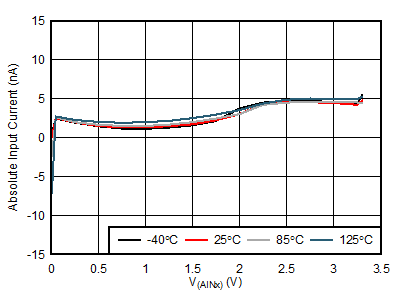
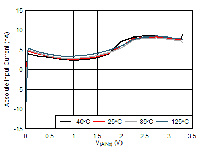
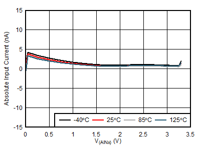
ADS112U04 D019_sbas752.gif
Normal mode, PGA disabled, VIN = 0 V
Figure 6. Absolute Input current vs Absolute Input Voltage
ADS112U04 D023_sbas752.gif
Turbo mode, PGA disabled, VIN = 0 V
Figure 8. Absolute Input Current vs Absolute Input Voltage
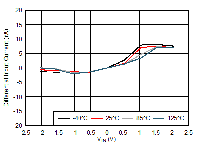
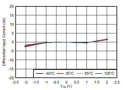
ADS112U04 D027_sbas752.gif
Normal mode, PGA disabled, VCM = 1.65 V
Figure 10. Differential Input Current vs
Differential Input Voltage
ADS112U04 D031_sbas752.gif
Turbo mode, PGA disabled, VCM = 1.65 V
Figure 12. Differential Input Current vs
Differential Input Voltage
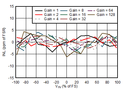
ADS112U04 D002_sbas752.gif
PGA enabled, external reference, best fit
Figure 14. INL vs Differential Input Voltage
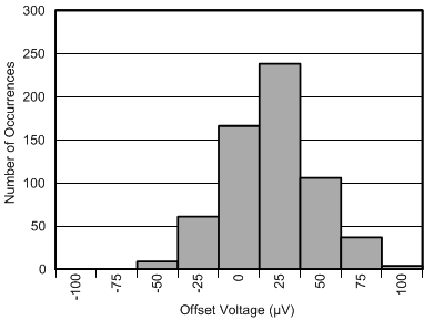
ADS112U04 D036_sbas752.gif
PGA enabled, gain = 1, 620 samples
Figure 16. Offset Voltage Histogram
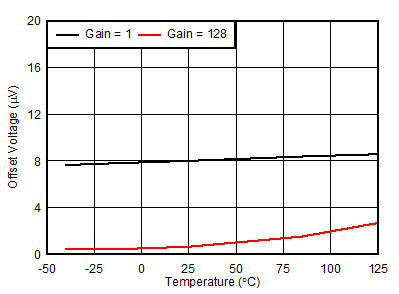
ADS112U04 D043_sbas752.gif
PGA enabled
Figure 18. Input Offset Voltage vs Temperature
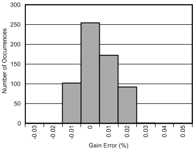
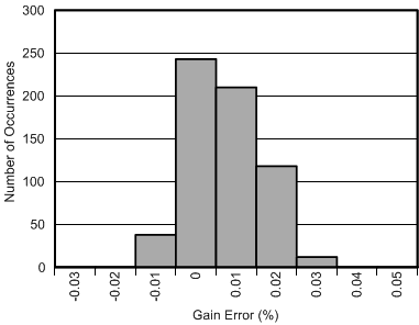
ADS112U04 D011_sbas752.gif
PGA enabled, gain = 1, 620 samples
Figure 20. Gain Error Histogram
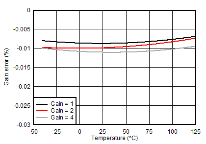
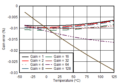
ADS112U04 D041_sbas752.gif
PGA disabled
Figure 22. Gain Error vs Temperature
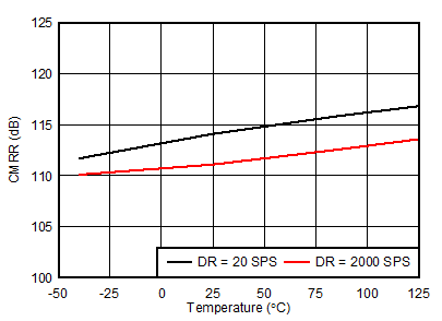
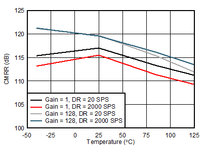
ADS112U04 D051_sbas752.gif
PGA disabled
Figure 24. DC CMRR vs Temperature
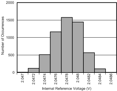
ADS112U04 D062_sbas752.gif
5940 samples, TSSOP package
Figure 26. Internal Reference Voltage Histogram
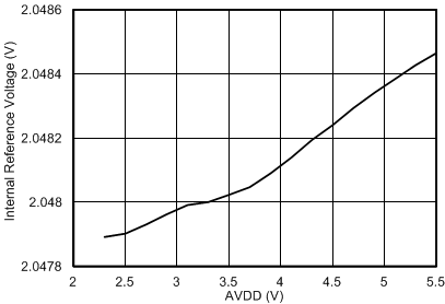
ADS112U04 D035_sbas752.gif
Figure 28. Internal Reference Voltage vs AVDD
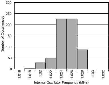
ADS112U04 D053_sbas752.gif
Normal mode
Figure 30. Internal Oscillator Frequency Histogram
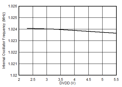
ADS112U04 D061_sbas752.gif
Normal mode
Figure 32. Internal Oscillator Frequency vs DVDD
ADS112U04 D064_sbas752.gif
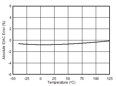
Figure 34. IDAC Accuracy vs Temperature
ADS112U04 D066_sbas752.gif
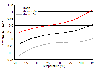
Figure 36. Internal Temperature Sensor Accuracy vs Temperature
ADS112U04 D007_sbas752.gif
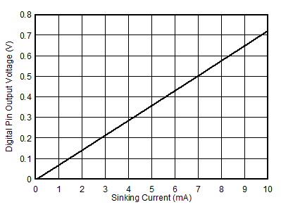
DVDD = 3.3 V
Figure 38. Digital Pin Output Voltage vs Sinking Current
ADS112U04 D045_sbas752.gif
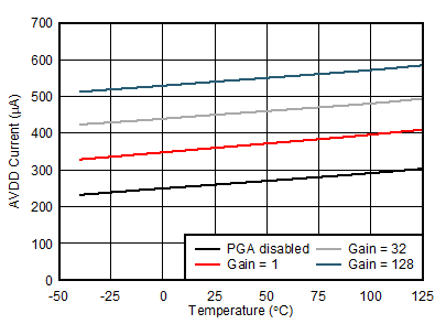
Normal mode
Figure 40. Analog Supply Current vs Temperature
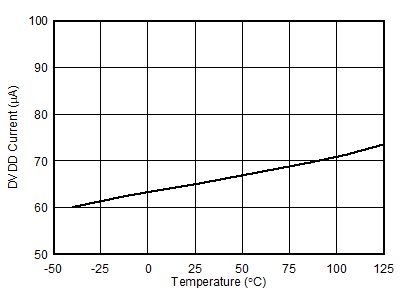
ADS112U04 D039_sbas752.gif
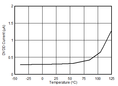
Power-down mode
Figure 42. Digital Supply Current vs Temperature
ADS112U04 D038_sbas752.gif
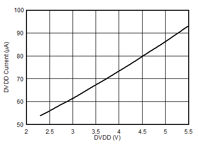
Normal mode
Figure 44. Digital Supply Current vs DVDD
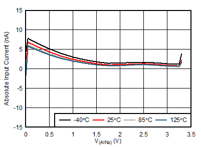
ADS112U04 D021_sbas752.gif
Normal mode, PGA enabled, VIN = 0 V
Figure 7. Absolute Input Current vs Absolute Input Voltage
ADS112U04 D025_sbas752.gif
Turbo mode, PGA enabled, VIN = 0 V
Figure 9. Absolute Input Current vs Absolute Input Voltage
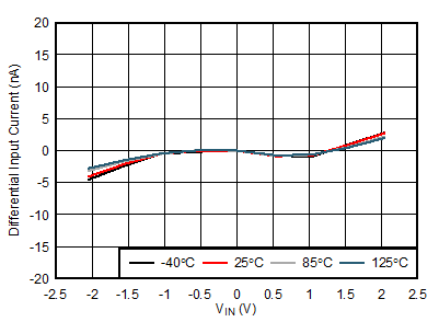
ADS112U04 D029_sbas752.gif
Normal mode, PGA enabled, VCM = 1.65 V
Figure 11. Differential Input Current vs
Differential Input Voltage
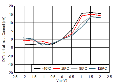
ADS112U04 D033_sbas752.gif
Turbo mode, PGA enabled, VCM = 1.65 V
Figure 13. Differential Input Current vs
Differential Input Voltage
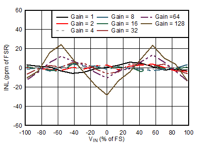
ADS112U04 D003_sbas752.gif
PGA enabled, internal reference, best fit
Figure 15. INL vs Differential Input Voltage
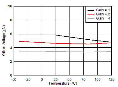
ADS112U04 D001_sbas752.gif
PGA disabled
Figure 17. Input Offset Voltage vs Temperature
ADS112U04 D008_sbas752.gif
PGA disabled, gain = 1, 620 samples
Figure 19. Gain Error Histogram
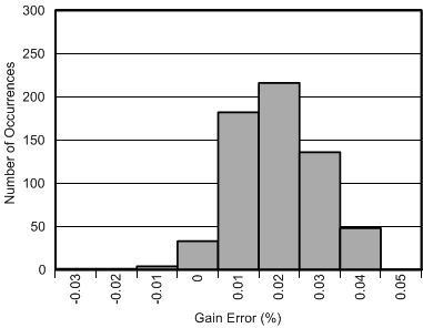
ADS112U04 D018_sbas752.gif
PGA enabled, gain = 128, 620 samples
Figure 21. Gain Error Histogram
ADS112U04 D042_sbas752.gif
PGA enabled
Figure 23. Gain Error vs Temperature
ADS112U04 D052_sbas752.gif
PGA enabled
Figure 25. DC CMRR vs Temperature
ADS112U04 D063_sbas752.gif
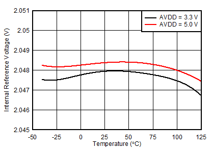
Figure 27. Internal Reference Voltage vs Temperature
ADS112U04 D059_sbas752.gif
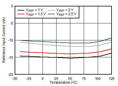
Figure 29. External Reference Input Current vs Temperature
ADS112U04 D060_sbas752.gif
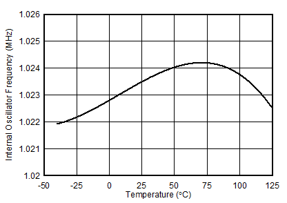
Normal mode
Figure 31. Internal Oscillator Frequency vs Temperature
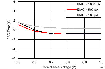
ADS112U04 C006_bas501.png
Figure 33. IDAC Accuracy vs Compliance Voltage
ADS112U04 D065_sbas752.gif
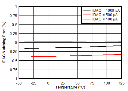
Figure 35. IDAC Matching vs Temperature
ADS112U04 D006_sbas752.gif
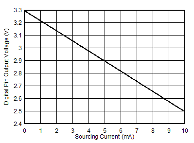
DVDD = 3.3 V
Figure 37. Digital Pin Output Voltage vs Sourcing Current
ADS112U04 D044_sbas752.gif
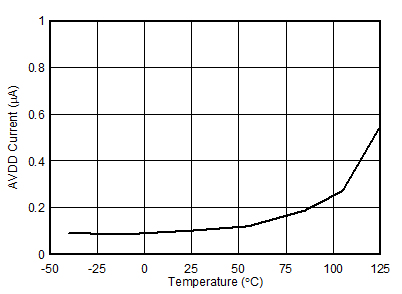
Power-down mode
Figure 39. Analog Supply Current vs Temperature
ADS112U04 D046_sbas752.gif
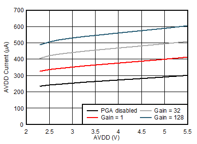
Normal mode
Figure 41. Analog Supply Current vs AVDD
ADS112U04 D040_sbas752.gif
Normal mode
Figure 43. Digital Supply Current vs Temperature