ZHCSHF4J May 2004 – January 2018 TPS51116
PRODUCTION DATA.
- 1 特性
- 2 应用
- 3 说明
- 4 修订历史记录
- 5 Pin Configuration and Functions
- 6 Specifications
-
7 Detailed Description
- 7.1 Overview
- 7.2 Functional Block Diagram
- 7.3
Feature Description
- 7.3.1 VDDQ SMPS, Light Load Condition
- 7.3.2 Low-Side Driver
- 7.3.3 High-Side Driver
- 7.3.4 Current Sensing Scheme
- 7.3.5 PWM Frequency and Adaptive On-Time Control
- 7.3.6 VDDQ Output Voltage Selection
- 7.3.7 VTT Linear Regulator and VTTREF
- 7.3.8 Controling Outputs Using the S3 and S5 Pins
- 7.3.9 Soft-Start Function and Powergood Status
- 7.3.10 VDDQ and VTT Discharge Control
- 7.3.11 Current Protection for VDDQ
- 7.3.12 Current Protection for VTT
- 7.3.13 Overvoltage and Undervoltage Protection for VDDQ
- 7.3.14 Undervoltage Lockout (UVLO) Protection, V5IN (PWP), V5FILT (RGE)
- 7.3.15 Input Capacitor, V5IN (PWP), V5FILT (RGE)
- 7.3.16 Thermal Shutdown
- 7.4 Device Functional Modes
- 8 Application and Implementation
- 9 Power Supply Recommendations
- 10Layout
- 11器件和文档支持
- 12机械、封装和可订购信息
7.3.7 VTT Linear Regulator and VTTREF
The TPS51116 device integrates high performance low-dropout linear regulator that is capable of sourcing and sinking current up to 3 A. This VTT linear regulator employs ultimate fast response feedback loop so that small ceramic capacitors are enough to keep tracking the VTTREF within ±40 mV at all conditions including fast load transient. To achieve tight regulation with minimum effect of wiring resistance, a remote sensing terminal, VTTSNS, should be connected to the positive node of VTT output capacitor(s) as a separate trace from VTT pin. For stable operation, total capacitance of the VTT output terminal can be equal to or greater than 20 μF. It is recommended to attach two 10-μF ceramic capacitors in parallel to minimize the effect of ESR and ESL. If ESR of the output capacitor is greater than 2 mΩ, insert an RC filter between the output and the VTTSNS input to achieve loop stability. The RC filter time constant should be almost the same or slightly lower than the time constant made by the output capacitor and its ESR. VTTREF block consists of on-chip 1/2 divider, LPF and buffer. This regulator also has sink and source capability up to 10 mA. Bypass VTTREF to GND by a 0.033-μF ceramic capacitor for stable operation.
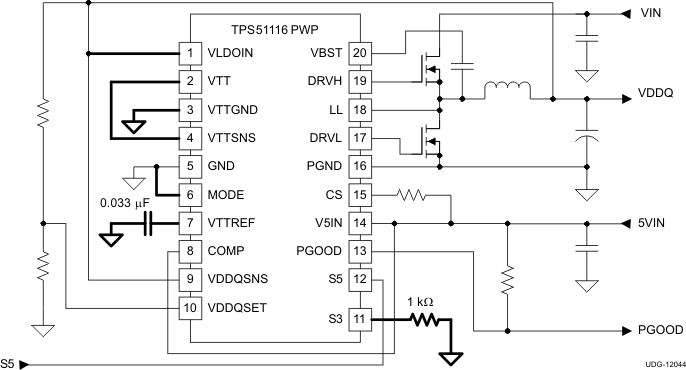
When VTT is not required in the design, following treatment is strongly recommended.
- Connect VLDOIN to VDDQSNS.
- Tie VTTSNS to VTT, and remove capacitors from VTT to float.
- Connect VTTGND and MODE to GND (Non-tracking discharge mode as shown in Table 3)
- Maintain a 0.033-µF capacitor connected at VTTREF.
- Pull down S3 to GND with 1 kΩ of resistance.
A typical circuit for this application is shown in Figure 34
 Figure 34. Application Circuit When VTT Is Not Required