ZHCSHF4J May 2004 – January 2018 TPS51116
PRODUCTION DATA.
- 1 特性
- 2 应用
- 3 说明
- 4 修订历史记录
- 5 Pin Configuration and Functions
- 6 Specifications
-
7 Detailed Description
- 7.1 Overview
- 7.2 Functional Block Diagram
- 7.3
Feature Description
- 7.3.1 VDDQ SMPS, Light Load Condition
- 7.3.2 Low-Side Driver
- 7.3.3 High-Side Driver
- 7.3.4 Current Sensing Scheme
- 7.3.5 PWM Frequency and Adaptive On-Time Control
- 7.3.6 VDDQ Output Voltage Selection
- 7.3.7 VTT Linear Regulator and VTTREF
- 7.3.8 Controling Outputs Using the S3 and S5 Pins
- 7.3.9 Soft-Start Function and Powergood Status
- 7.3.10 VDDQ and VTT Discharge Control
- 7.3.11 Current Protection for VDDQ
- 7.3.12 Current Protection for VTT
- 7.3.13 Overvoltage and Undervoltage Protection for VDDQ
- 7.3.14 Undervoltage Lockout (UVLO) Protection, V5IN (PWP), V5FILT (RGE)
- 7.3.15 Input Capacitor, V5IN (PWP), V5FILT (RGE)
- 7.3.16 Thermal Shutdown
- 7.4 Device Functional Modes
- 8 Application and Implementation
- 9 Power Supply Recommendations
- 10Layout
- 11器件和文档支持
- 12机械、封装和可订购信息
7.3.9 Soft-Start Function and Powergood Status
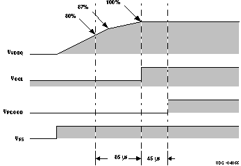
The soft-start function of the SMPS is achieved by ramping up reference voltage and two-stage current clamp. At the starting point, the reference voltage is set to 650 mV (87% of its target value) and the overcurrent threshold is set half of the nominal value. When UVP comparator detects VDDQ become greater than 80% of the target, the reference voltage is raised toward 750 mV using internal 4-bit DAC. This takes approximately 85 μs. The overcurrent threshold is released to nominal value at the end of this period. The powergood signal waits another 45 μs after the reference voltage reaches 750 mV and the VDDQ voltage becomes good (above 95% of the target voltage), then turns off powergood open-drain MOSFET.
The soft-start function of the VTT LDO is achieved by current clamp. The current limit threshold is also changed in two stages using an internal powergood signal dedicated for LDO. During VTT is below the powergood threshold, the current limit level is cut into 60% (2.2 A).This allows the output capacitors to be charged with low and constant current that gives linear ramp up of the output. When the output comes up to the good state, the overcurrent limit level is released to normal value (3.8 A). The device has an independent counter for each output, but the PGOOD signal indicates the status of VDDQ only and does not indicate VTT powergood status externally. See Figure 35.
 Figure 35. VDDQ Soft-Start and Powergood Timing
Soft-start duration, tVDDQSS, tVTTSS are functions of output capacitances.

where
- IVTTOCL = 2.2 A (typ)
In both Equation 2 and Equation 3 , no load current during start-up are assumed. Note that both switchers and the LDO do not start up with full load condition.
