ZHCSHF4J May 2004 – January 2018 TPS51116
PRODUCTION DATA.
- 1 特性
- 2 应用
- 3 说明
- 4 修订历史记录
- 5 Pin Configuration and Functions
- 6 Specifications
-
7 Detailed Description
- 7.1 Overview
- 7.2 Functional Block Diagram
- 7.3
Feature Description
- 7.3.1 VDDQ SMPS, Light Load Condition
- 7.3.2 Low-Side Driver
- 7.3.3 High-Side Driver
- 7.3.4 Current Sensing Scheme
- 7.3.5 PWM Frequency and Adaptive On-Time Control
- 7.3.6 VDDQ Output Voltage Selection
- 7.3.7 VTT Linear Regulator and VTTREF
- 7.3.8 Controling Outputs Using the S3 and S5 Pins
- 7.3.9 Soft-Start Function and Powergood Status
- 7.3.10 VDDQ and VTT Discharge Control
- 7.3.11 Current Protection for VDDQ
- 7.3.12 Current Protection for VTT
- 7.3.13 Overvoltage and Undervoltage Protection for VDDQ
- 7.3.14 Undervoltage Lockout (UVLO) Protection, V5IN (PWP), V5FILT (RGE)
- 7.3.15 Input Capacitor, V5IN (PWP), V5FILT (RGE)
- 7.3.16 Thermal Shutdown
- 7.4 Device Functional Modes
- 8 Application and Implementation
- 9 Power Supply Recommendations
- 10Layout
- 11器件和文档支持
- 12机械、封装和可订购信息
7.4.3 D-CAP™ Mode Operation
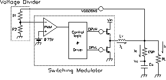
Figure 37 shows a simplified schematic of a buck converter application operating in D-CAP™ mode.
 Figure 37. Linearizing the Modulator
The PWM comparator compares the VDDQSNS voltage divided by R1 and R2 with internal reference voltage, and determines the timing to turn on the high-side MOSFET. The gain and speed of the comparator is high enough to maintain the voltage at the beginning of each on cycle (or the end of off cycle) substantially constant. The DC output voltage may have line regulation due to ripple amplitude that slightly increases as the input voltage increase.
f0, must be lower than 1/3 of the switching frequency.Equation 16 defines the 0-dB frequency calculation.

Because the 0-dB frequency, f0 is determined solely by the output capacitor characteristics, loop stability of D-CAP™ mode is determined by the capacitor’s chemistry. For example, specialty polymer capacitors (SP-CAP) have CO in the order of several 100 μF and ESR in range of 10 mΩ. These makes f0 on the order of 100 kHz or less and the loop is then stable. However, ceramic capacitors have f0 at more than 700 kHz, which is not suitable for this operational mode.
Although D-CAP™ mode design provides many advantages such as ease-of-use, minimum external components configuration and extremely short response time, due to not employing an error amplifier in the loop, sufficient amount of feedback signal needs to be provided by external circuit to reduce jitter level.
The required signal level is approximately 15 mV at comparing point. This gives VRIPPLE = (VOUT/0.75) x 15 (mV) at the output node. The output capacitor’s ESR should meet this requirement.
The external components selection is simple for applications that operate in D-CAP™ mode.
- Choose inductor. Inductor selection for DCAP mode operation is the same as for current mode operation. Please refer to the instructions in the Current Mode Operation section.
- Choose output capacitor(s).Organic semiconductor capacitor(s) or specialty polymer capacitor(s) are recommended. Determine ESR to meet required ripple voltage above. Equation 17 shows an approximation calculation.
