ZHCSHF4J May 2004 – January 2018 TPS51116
PRODUCTION DATA.
- 1 特性
- 2 应用
- 3 说明
- 4 修订历史记录
- 5 Pin Configuration and Functions
- 6 Specifications
-
7 Detailed Description
- 7.1 Overview
- 7.2 Functional Block Diagram
- 7.3
Feature Description
- 7.3.1 VDDQ SMPS, Light Load Condition
- 7.3.2 Low-Side Driver
- 7.3.3 High-Side Driver
- 7.3.4 Current Sensing Scheme
- 7.3.5 PWM Frequency and Adaptive On-Time Control
- 7.3.6 VDDQ Output Voltage Selection
- 7.3.7 VTT Linear Regulator and VTTREF
- 7.3.8 Controling Outputs Using the S3 and S5 Pins
- 7.3.9 Soft-Start Function and Powergood Status
- 7.3.10 VDDQ and VTT Discharge Control
- 7.3.11 Current Protection for VDDQ
- 7.3.12 Current Protection for VTT
- 7.3.13 Overvoltage and Undervoltage Protection for VDDQ
- 7.3.14 Undervoltage Lockout (UVLO) Protection, V5IN (PWP), V5FILT (RGE)
- 7.3.15 Input Capacitor, V5IN (PWP), V5FILT (RGE)
- 7.3.16 Thermal Shutdown
- 7.4 Device Functional Modes
- 8 Application and Implementation
- 9 Power Supply Recommendations
- 10Layout
- 11器件和文档支持
- 12机械、封装和可订购信息
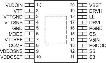
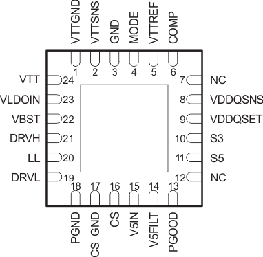
5 Pin Configuration and Functions
PWP Package
20-Pin HTSSOP
Top View

RGE Package
24-Pin QFN
Top View

Pin Functions
| NAME | NO. | I/O | DESCRIPTION | |
|---|---|---|---|---|
| PWP | RGE | |||
| COMP | 8 | 6 | I/O | Output of the transconductance amplifier for phase compensation. Connect to V5IN pin to disable gM amplifier and use D-CAP mode. |
| CS | 15 | 16 | I/O | Current sense comparator input (-) for resistor current sense scheme. Or overcurrent trip voltage setting input for RDS(on) current sense scheme if connected to V5IN (PWP), V5FILT (RGE) through the voltage setting resistor. |
| DRVH | 19 | 21 | O | Switching (high-side) MOSFET gate-drive output. |
| DRVL | 17 | 19 | O | Rectifying (low-side) MOSFET gate-drive output. |
| GND | 5 | 3 | - | Signal ground. Connect to negative terminal of the VTT LDO output capacitor. |
| CS_GND | - | 17 | – | Current sense comparator input (+) and ground for powergood circuit. |
| LL | 18 | 20 | I/O | Switching (high-side) MOSFET gate driver return. Current sense comparator input (-) for RDS(on) current sense. |
| MODE | 6 | 4 | I | Discharge mode setting pin. See VDDQ and VTT Discharge Control section. |
| NC | – | 7 | – | No connect. |
| – | 12 | – | ||
| PGND | 16 | 18 | – | Ground for rectifying (low-side) MOSFET gate driver (PWP, RGE). Also current sense comparator input(+) and ground for powergood circuit (PWP). |
| PGOOD | 13 | 13 | O | Powergood signal open drain output, In HIGH state when VDDQ output voltage is within the target range. |
| S3 | 11 | 10 | I | S3 signal input. |
| S5 | 12 | 11 | I | S5 signal input. |
| V5IN | 14 | 15 | I | 5-V power supply input for internal circuits (PWP) and MOSFET gate drivers (PWP, RGE). |
| V5FILT | – | 14 | I | Filtered 5-V power supply input for internal circuits. Connect R-C network from V5IN to V5FILT. |
| VBST | 20 | 22 | I/O | Switching (high-side) MOSFET driver bootstrap voltage input. |
| VDDQSET | 10 | 9 | I | VDDQ output voltage setting pin. See VDDQ Output Voltage Selection section. |
| VDDQSNS | 9 | 8 | I/O | VDDQ reference input for VTT and VTTREF. Power supply for the VTTREF. Discharge current sinking terminal for VDDQ Non-tracking discharge. Output voltage feedback input for VDDQ output if VDDQSET pin is connected to V5IN or GND. |
| VLDOIN | 1 | 23 | I | Power supply for the VTT LDO. |
| VTT | 2 | 24 | O | Power output for the VTT LDO. |
| VTTGND | 3 | 1 | - | Power ground output for the VTT LDO. |
| VTTREF | 7 | 5 | O | VTTREF buffered reference output. |
| VTTSNS | 4 | 2 | I | Voltage sense input for the VTT LDO. Connect to plus terminal of the VTT LDO output capacitor. |