ZHCSHG7C January 2018 – July 2018 TPSM84209
PRODUCTION DATA.
- 1 特性
- 2 应用
- 3 说明
- 4 修订历史记录
- 5 Pin Configuration and Functions
- 6 Specifications
-
7 Detailed Description
- 7.1 Overview
- 7.2 Functional Block Diagram
- 7.3
Feature Description
- 7.3.1 Adjusting the Output Voltage
- 7.3.2 Input Capacitor Selection
- 7.3.3 Undervoltage Lockout (UVLO)
- 7.3.4 Output Capacitor Selection
- 7.3.5 Feed-Forward Capacitor
- 7.3.6 Operating Range
- 7.3.7 Output Current Rating
- 7.3.8 Enable (EN)
- 7.3.9 Internal Soft Start
- 7.3.10 Safe Start-Up Into Prebiased Outputs
- 7.3.11 Light Load Efficiency / Eco-Mode
- 7.3.12 Voltage Dropout
- 7.3.13 Overcurrent Protection
- 7.3.14 Output Overvoltage Protection (OVP)
- 7.3.15 Thermal Performance
- 7.3.16 Thermal Shutdown
- 7.4 Device Functional Modes
- 8 Application and Implementation
- 9 Power Supply Recommendations
- 10Layout
- 11器件和文档支持
- 12机械、封装和可订购信息
7.3.3 Undervoltage Lockout (UVLO)
The TPSM84209 device has an internal UVLO circuit which prevents the device from operating until the VIN voltage exceeds the UVLO rising threshold, (4.1 V (typical)). The device is disabled when the VIN pin voltage falls below the internal VIN UVLO threshold. The internal VIN UVLO threshold has a hysteresis of 500 mV.
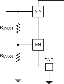
Applications may require a higher UVLO threshold to prevent early turnon, for sequencing requirements or to prevent input current draw at lower input voltages. An external resistor divider can be added to the EN pin to adjust the UVLO threshold higher. The external resistor divider can be configured as shown in Figure 18. Table 3 lists standard values for RUVLO1 and RUVLO2 to adjust the UVLO voltage higher.
 Figure 18. Adjustable UVLO
 Table 3. Standard Resistor Values for Adjusting UVLO
| VIN UVLO (V) | 4.5 | 10 | 15 | 18 | 20 |
|---|---|---|---|---|---|
| RUVLO1 (kΩ) | 68.1 | 68.1 | 68.1 | 68.1 | 68.1 |
| RUVLO2 (kΩ) | 25.5 | 9.53 | 6.04 | 4.99 | 4.42 |