ZHCSHG7C January 2018 – July 2018 TPSM84209
PRODUCTION DATA.
- 1 特性
- 2 应用
- 3 说明
- 4 修订历史记录
- 5 Pin Configuration and Functions
- 6 Specifications
-
7 Detailed Description
- 7.1 Overview
- 7.2 Functional Block Diagram
- 7.3
Feature Description
- 7.3.1 Adjusting the Output Voltage
- 7.3.2 Input Capacitor Selection
- 7.3.3 Undervoltage Lockout (UVLO)
- 7.3.4 Output Capacitor Selection
- 7.3.5 Feed-Forward Capacitor
- 7.3.6 Operating Range
- 7.3.7 Output Current Rating
- 7.3.8 Enable (EN)
- 7.3.9 Internal Soft Start
- 7.3.10 Safe Start-Up Into Prebiased Outputs
- 7.3.11 Light Load Efficiency / Eco-Mode
- 7.3.12 Voltage Dropout
- 7.3.13 Overcurrent Protection
- 7.3.14 Output Overvoltage Protection (OVP)
- 7.3.15 Thermal Performance
- 7.3.16 Thermal Shutdown
- 7.4 Device Functional Modes
- 8 Application and Implementation
- 9 Power Supply Recommendations
- 10Layout
- 11器件和文档支持
- 12机械、封装和可订购信息
5 Pin Configuration and Functions
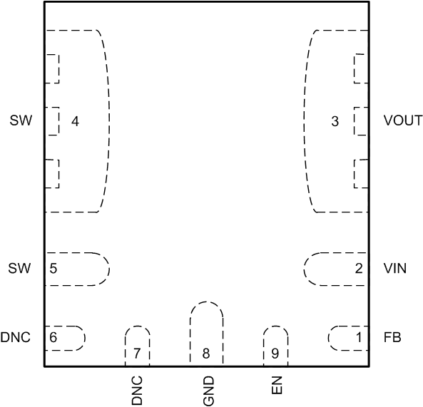
RKH Package
9-Pin QFN
Top View

Pin Functions
| PIN | TYPE (1) | DESCRIPTION | |
|---|---|---|---|
| NAME | NO. | ||
| DNC | 6, 7 | — | Do Not Connect. Do not connect these pins to GND or to any other voltage. These pins are connected to internal circuitry. Each pin must be soldered to an isolated pad. |
| EN | 9 | I | Enable pin. An open drain/collector device can be used to control the EN function. The module is disabled when this pin is pulled low. This pin can also be connected to an external resistor divider connected between VIN and GND to adjust the UVLO above the internal default setting. Float this pin when not used. |
| FB | 1 | I | Feedback input. To adjust the output voltage connect this pin to the center point of an external resistor divider connected between VOUT and GND. |
| GND | 8 | G | Ground pin. This is the return current path for the device. Connect this pin to the input source return, the load return, and to the ground side of the VIN and VOUT bypass capacitors using power ground planes on the PCB. |
| SW | 4, 5 | O | Switch node. These pins are connected to the input side of the internal output inductor. Do not place any external components on these pins or tie them to a pin of another function. |
| VIN | 2 | I | Input voltage. Connect this pin to the input source and connect external bypass capacitors between this pin and GND, close to the module. |
| VOUT | 3 | O | Output voltage. This pin is connected to the internal output inductor. Connect this pin to the output load and connect external bypass capacitors between this pin and GND close to the module. |
(1) G = Ground, I = Input, O = Output