ZHCSHN9A February   2018  – April 2018 LMK05028

PRODUCTION DATA.  

  1. 特性
  2. 应用
  3. 说明
    1.     Device Images
      1.      简化方框图
  4. 修订历史记录
  5. 说明 (续)
  6. Pin Configuration and Functions
    1.     Pin Functions
    2. 6.1 Device Start-Up Modes
  7. Specifications
    1. 7.1 Absolute Maximum Ratings
    2. 7.2 ESD Ratings
    3. 7.3 Recommended Operating Conditions
    4. 7.4 Thermal Information
    5. 7.5 Electrical Characteristics
    6. 7.6 Timing Diagrams
    7. 7.7 Typical Characteristics
  8. Parameter Measurement Information
    1. 8.1 Output Clock Test Configurations
  9. Detailed Description
    1. 9.1 Overview
      1. 9.1.1 ITU-T G.8262 (SyncE) Standards Compliance
    2. 9.2 Functional Block Diagrams
      1. 9.2.1 PLL Architecture Overview
      2. 9.2.2 3-Loop Mode
        1. 9.2.2.1 PLL Output Clock Phase Noise Analysis in 3-Loop Mode
      3. 9.2.3 2-Loop REF-DPLL Mode
      4. 9.2.4 2-Loop TCXO-DPLL Mode
      5. 9.2.5 PLL Configurations for Common Applications
    3. 9.3 Feature Description
      1. 9.3.1  Oscillator Input (XO_P/N)
      2. 9.3.2  TCXO/OCXO Input (TCXO_IN)
      3. 9.3.3  Reference Inputs (INx_P/N)
      4. 9.3.4  Clock Input Interfacing and Termination
      5. 9.3.5  Reference Input Mux Selection
        1. 9.3.5.1 Automatic Input Selection
        2. 9.3.5.2 Manual Input Selection
      6. 9.3.6  Hitless Switching
      7. 9.3.7  Gapped Clock Support on Reference Inputs
      8. 9.3.8  Input Clock and PLL Monitoring, Status, and Interrupts
        1. 9.3.8.1 XO Input Monitoring
        2. 9.3.8.2 TCXO Input Monitoring
        3. 9.3.8.3 Reference Input Monitoring
          1. 9.3.8.3.1 Reference Validation Timer
          2. 9.3.8.3.2 Amplitude Monitor
          3. 9.3.8.3.3 Missing Pulse Monitor (Late Detect)
          4. 9.3.8.3.4 Runt Pulse Monitor (Early Detect)
          5. 9.3.8.3.5 Frequency Monitoring
          6. 9.3.8.3.6 Phase Valid Monitor for 1-PPS Inputs
        4. 9.3.8.4 PLL Lock Detectors
        5. 9.3.8.5 Tuning Word History
        6. 9.3.8.6 Status Outputs
        7. 9.3.8.7 Interrupt
      9. 9.3.9  PLL Channels
        1. 9.3.9.1  PLL Frequency Relationships
        2. 9.3.9.2  Analog PLL (APLL)
        3. 9.3.9.3  APLL XO Doubler
        4. 9.3.9.4  APLL Phase Frequency Detector (PFD) and Charge Pump
        5. 9.3.9.5  APLL Loop Filter
        6. 9.3.9.6  APLL Voltage Controlled Oscillator (VCO)
          1. 9.3.9.6.1 VCO Calibration
        7. 9.3.9.7  APLL VCO Post-Dividers (P1, P2)
        8. 9.3.9.8  APLL Fractional N Divider (N) With SDM
        9. 9.3.9.9  REF-DPLL Reference Divider (R)
        10. 9.3.9.10 TCXO/OCXO Input Doubler and M Divider
        11. 9.3.9.11 TCXO Mux
        12. 9.3.9.12 REF-DPLL and TCXO-DPLL Time-to-Digital Converter (TDC)
        13. 9.3.9.13 REF-DPLL and TCXO-DPLL Loop Filter
        14. 9.3.9.14 REF-DPLL and TCXO-DPLL Feedback Dividers
      10. 9.3.10 Output Clock Distribution
      11. 9.3.11 Output Channel Muxes
        1. 9.3.11.1 TCXO/Ref Bypass Mux
      12. 9.3.12 Output Dividers
      13. 9.3.13 Clock Outputs (OUTx_P/N)
        1. 9.3.13.1 AC-Differential Output (AC-DIFF)
        2. 9.3.13.2 HCSL Output
        3. 9.3.13.3 LVCMOS Output (1.8 V, 2.5 V)
        4. 9.3.13.4 Output Auto-Mute During LOL or LOS
      14. 9.3.14 Glitchless Output Clock Start-Up
      15. 9.3.15 Clock Output Interfacing and Termination
      16. 9.3.16 Output Synchronization (SYNC)
      17. 9.3.17 Zero-Delay Mode (ZDM) Configuration
      18. 9.3.18 PLL Cascading With Internal VCO Loopback
    4. 9.4 Device Functional Modes
      1. 9.4.1 Device Start-Up Modes
        1. 9.4.1.1 EEPROM Mode
        2. 9.4.1.2 ROM Mode
      2. 9.4.2 PLL Operating Modes
        1. 9.4.2.1 Free-Run Mode
        2. 9.4.2.2 Lock Acquisition
        3. 9.4.2.3 Locked Mode
        4. 9.4.2.4 Holdover Mode
      3. 9.4.3 PLL Start-Up Sequence
      4. 9.4.4 Digitally-Controlled Oscillator (DCO) Mode
        1. 9.4.4.1 DCO Frequency Step Size
        2. 9.4.4.2 DCO Direct-Write Mode
      5. 9.4.5 Zero-Delay Mode (ZDM)
      6. 9.4.6 Cascaded PLL Operation
    5. 9.5 Programming
      1. 9.5.1 Interface and Control
      2. 9.5.2 I2C Serial Interface
        1. 9.5.2.1 I2C Block Register Transfers
      3. 9.5.3 SPI Serial Interface
        1. 9.5.3.1 SPI Block Register Transfer
      4. 9.5.4 Register Map Generation
      5. 9.5.5 General Register Programming Sequence
      6. 9.5.6 EEPROM Programming Flow
        1. 9.5.6.1 EEPROM Programming Using Register Commit (Method #1)
          1. 9.5.6.1.1 Write SRAM Using Register Commit
          2. 9.5.6.1.2 Program EEPROM
        2. 9.5.6.2 EEPROM Programming Using Direct SRAM Writes (Method #2)
          1. 9.5.6.2.1 Write SRAM Using Direct Writes
      7. 9.5.7 Read SRAM
      8. 9.5.8 Read EEPROM
      9. 9.5.9 EEPROM Start-Up Mode Default Configuration
    6. 9.6 Register Maps
  10. 10Application and Implementation
    1. 10.1 Application Information
      1. 10.1.1 Device Start-Up Sequence
      2. 10.1.2 Power Down (PDN) Pin
      3. 10.1.3 Power Rail Sequencing, Power Supply Ramp Rate, and Mixing Supply Domains
        1. 10.1.3.1 Mixing Supplies
        2. 10.1.3.2 Power-On Reset (POR) Circuit
        3. 10.1.3.3 Powering Up From a Single-Supply Rail
        4. 10.1.3.4 Power Up From Split-Supply Rails
        5. 10.1.3.5 Non-Monotonic or Slow Power-Up Supply Ramp
      4. 10.1.4 Slow or Delayed XO Start-Up
    2. 10.2 Typical Application
      1. 10.2.1 Design Requirements
      2. 10.2.2 Detailed Design Procedure
      3. 10.2.3 Application Curves
    3. 10.3 Do's and Don'ts
  11. 11Power Supply Recommendations
    1. 11.1 Power Supply Bypassing
  12. 12Layout
    1. 12.1 Layout Guidelines
    2. 12.2 Layout Example
    3. 12.3 Thermal Reliability
  13. 13器件和文档支持
    1. 13.1 器件支持
      1. 13.1.1 时钟架构
      2. 13.1.2 TICS Pro
    2. 13.2 文档支持
      1. 13.2.1 相关文档
    3. 13.3 接收文档更新通知
    4. 13.4 社区资源
    5. 13.5 商标
    6. 13.6 静电放电警告
    7. 13.7 术语表
  14. 14机械、封装和可订购信息

PLL Architecture Overview

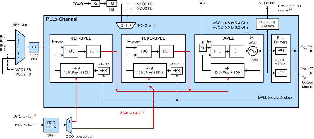
Figure 19 shows the 3-loop architecture implemented the same for both PLL channels with exception of the VCO frequency range. Each channel has three phase-locked loops with two digital PLLs (REF-DPLL and TCXO-DPLL) and one analog PLL (APLL) with integrated VCO. The REF-DPLL and TCXO-DPLL are each comprised of a time-to-digital converter (TDC), digital loop filter (DLF), feedback prescaler (PR), and 40-bit fractional feedback (FB) divider with sigma-delta-modulator (SDM or "MASH"). The APLL is comprised of a reference frequency doubler (×2), phase-frequency detector (PFD), loop filter (LF), fractional feedback (N) divider with SDM, and VCO.
LMK05028 lmk05028-pll-core-generic-fbd.gif
Fractional divider SDM control node depends on the selected PLL mode configuration.
DCO frequency adjustments can be software or pin controlled.
PLL cascading options: a) PLL1 VCO1 Loopback to PLL2, b) PLL2 VCO2 Loopback to PLL1.
Figure 19. PLL Architecture (One Channel)

Table 2 summarizes the PLL mode configuration options available in each channel. These modes support a wide range of use cases depending to the clock functionality and performance required in the application. Most applications will use 2-loop REF-DPLL or 3-loop mode for network synchronization clock features such as programmable loop bandwidth for jitter and wander attenuation, hitless switching, precise digital holdover, DCO frequency steering, and/or zero delay mode.

Table 2. PLL Mode Configuration Options

PLL MODE FRACTIONAL SDM ENABLED (SDM CONTROL FROM) DCO MODE OPTION FREE-RUN / HOLDOVER CLOCK
REF-DPLL TCXO-DPLL APLL
1-Loop (APLL only) Y (Free-run from XO) XO
2-Loop REF-DPLL Y (DCO option) Y (REF-DPLL) REF-DPLL SDM XO
2-Loop TCXO-DPLL Y (DCO option) Y (TCXO-DPLL) TCXO-DPLL SDM TCXO
3-Loop Y (DCO option) Y (REF-DPLL) Y (TCXO-DPLL) REF-DPLL SDM TCXO

The following sections describe the basic principle of operation for 2-loop and 3-loop modes. See PLL Operating Modes for more details on the PLL modes of operation including holdover.