ZHCSHN9A February   2018  – April 2018 LMK05028

PRODUCTION DATA.  

  1. 特性
  2. 应用
  3. 说明
    1.     Device Images
      1.      简化方框图
  4. 修订历史记录
  5. 说明 (续)
  6. Pin Configuration and Functions
    1.     Pin Functions
    2. 6.1 Device Start-Up Modes
  7. Specifications
    1. 7.1 Absolute Maximum Ratings
    2. 7.2 ESD Ratings
    3. 7.3 Recommended Operating Conditions
    4. 7.4 Thermal Information
    5. 7.5 Electrical Characteristics
    6. 7.6 Timing Diagrams
    7. 7.7 Typical Characteristics
  8. Parameter Measurement Information
    1. 8.1 Output Clock Test Configurations
  9. Detailed Description
    1. 9.1 Overview
      1. 9.1.1 ITU-T G.8262 (SyncE) Standards Compliance
    2. 9.2 Functional Block Diagrams
      1. 9.2.1 PLL Architecture Overview
      2. 9.2.2 3-Loop Mode
        1. 9.2.2.1 PLL Output Clock Phase Noise Analysis in 3-Loop Mode
      3. 9.2.3 2-Loop REF-DPLL Mode
      4. 9.2.4 2-Loop TCXO-DPLL Mode
      5. 9.2.5 PLL Configurations for Common Applications
    3. 9.3 Feature Description
      1. 9.3.1  Oscillator Input (XO_P/N)
      2. 9.3.2  TCXO/OCXO Input (TCXO_IN)
      3. 9.3.3  Reference Inputs (INx_P/N)
      4. 9.3.4  Clock Input Interfacing and Termination
      5. 9.3.5  Reference Input Mux Selection
        1. 9.3.5.1 Automatic Input Selection
        2. 9.3.5.2 Manual Input Selection
      6. 9.3.6  Hitless Switching
      7. 9.3.7  Gapped Clock Support on Reference Inputs
      8. 9.3.8  Input Clock and PLL Monitoring, Status, and Interrupts
        1. 9.3.8.1 XO Input Monitoring
        2. 9.3.8.2 TCXO Input Monitoring
        3. 9.3.8.3 Reference Input Monitoring
          1. 9.3.8.3.1 Reference Validation Timer
          2. 9.3.8.3.2 Amplitude Monitor
          3. 9.3.8.3.3 Missing Pulse Monitor (Late Detect)
          4. 9.3.8.3.4 Runt Pulse Monitor (Early Detect)
          5. 9.3.8.3.5 Frequency Monitoring
          6. 9.3.8.3.6 Phase Valid Monitor for 1-PPS Inputs
        4. 9.3.8.4 PLL Lock Detectors
        5. 9.3.8.5 Tuning Word History
        6. 9.3.8.6 Status Outputs
        7. 9.3.8.7 Interrupt
      9. 9.3.9  PLL Channels
        1. 9.3.9.1  PLL Frequency Relationships
        2. 9.3.9.2  Analog PLL (APLL)
        3. 9.3.9.3  APLL XO Doubler
        4. 9.3.9.4  APLL Phase Frequency Detector (PFD) and Charge Pump
        5. 9.3.9.5  APLL Loop Filter
        6. 9.3.9.6  APLL Voltage Controlled Oscillator (VCO)
          1. 9.3.9.6.1 VCO Calibration
        7. 9.3.9.7  APLL VCO Post-Dividers (P1, P2)
        8. 9.3.9.8  APLL Fractional N Divider (N) With SDM
        9. 9.3.9.9  REF-DPLL Reference Divider (R)
        10. 9.3.9.10 TCXO/OCXO Input Doubler and M Divider
        11. 9.3.9.11 TCXO Mux
        12. 9.3.9.12 REF-DPLL and TCXO-DPLL Time-to-Digital Converter (TDC)
        13. 9.3.9.13 REF-DPLL and TCXO-DPLL Loop Filter
        14. 9.3.9.14 REF-DPLL and TCXO-DPLL Feedback Dividers
      10. 9.3.10 Output Clock Distribution
      11. 9.3.11 Output Channel Muxes
        1. 9.3.11.1 TCXO/Ref Bypass Mux
      12. 9.3.12 Output Dividers
      13. 9.3.13 Clock Outputs (OUTx_P/N)
        1. 9.3.13.1 AC-Differential Output (AC-DIFF)
        2. 9.3.13.2 HCSL Output
        3. 9.3.13.3 LVCMOS Output (1.8 V, 2.5 V)
        4. 9.3.13.4 Output Auto-Mute During LOL or LOS
      14. 9.3.14 Glitchless Output Clock Start-Up
      15. 9.3.15 Clock Output Interfacing and Termination
      16. 9.3.16 Output Synchronization (SYNC)
      17. 9.3.17 Zero-Delay Mode (ZDM) Configuration
      18. 9.3.18 PLL Cascading With Internal VCO Loopback
    4. 9.4 Device Functional Modes
      1. 9.4.1 Device Start-Up Modes
        1. 9.4.1.1 EEPROM Mode
        2. 9.4.1.2 ROM Mode
      2. 9.4.2 PLL Operating Modes
        1. 9.4.2.1 Free-Run Mode
        2. 9.4.2.2 Lock Acquisition
        3. 9.4.2.3 Locked Mode
        4. 9.4.2.4 Holdover Mode
      3. 9.4.3 PLL Start-Up Sequence
      4. 9.4.4 Digitally-Controlled Oscillator (DCO) Mode
        1. 9.4.4.1 DCO Frequency Step Size
        2. 9.4.4.2 DCO Direct-Write Mode
      5. 9.4.5 Zero-Delay Mode (ZDM)
      6. 9.4.6 Cascaded PLL Operation
    5. 9.5 Programming
      1. 9.5.1 Interface and Control
      2. 9.5.2 I2C Serial Interface
        1. 9.5.2.1 I2C Block Register Transfers
      3. 9.5.3 SPI Serial Interface
        1. 9.5.3.1 SPI Block Register Transfer
      4. 9.5.4 Register Map Generation
      5. 9.5.5 General Register Programming Sequence
      6. 9.5.6 EEPROM Programming Flow
        1. 9.5.6.1 EEPROM Programming Using Register Commit (Method #1)
          1. 9.5.6.1.1 Write SRAM Using Register Commit
          2. 9.5.6.1.2 Program EEPROM
        2. 9.5.6.2 EEPROM Programming Using Direct SRAM Writes (Method #2)
          1. 9.5.6.2.1 Write SRAM Using Direct Writes
      7. 9.5.7 Read SRAM
      8. 9.5.8 Read EEPROM
      9. 9.5.9 EEPROM Start-Up Mode Default Configuration
    6. 9.6 Register Maps
  10. 10Application and Implementation
    1. 10.1 Application Information
      1. 10.1.1 Device Start-Up Sequence
      2. 10.1.2 Power Down (PDN) Pin
      3. 10.1.3 Power Rail Sequencing, Power Supply Ramp Rate, and Mixing Supply Domains
        1. 10.1.3.1 Mixing Supplies
        2. 10.1.3.2 Power-On Reset (POR) Circuit
        3. 10.1.3.3 Powering Up From a Single-Supply Rail
        4. 10.1.3.4 Power Up From Split-Supply Rails
        5. 10.1.3.5 Non-Monotonic or Slow Power-Up Supply Ramp
      4. 10.1.4 Slow or Delayed XO Start-Up
    2. 10.2 Typical Application
      1. 10.2.1 Design Requirements
      2. 10.2.2 Detailed Design Procedure
      3. 10.2.3 Application Curves
    3. 10.3 Do's and Don'ts
  11. 11Power Supply Recommendations
    1. 11.1 Power Supply Bypassing
  12. 12Layout
    1. 12.1 Layout Guidelines
    2. 12.2 Layout Example
    3. 12.3 Thermal Reliability
  13. 13器件和文档支持
    1. 13.1 器件支持
      1. 13.1.1 时钟架构
      2. 13.1.2 TICS Pro
    2. 13.2 文档支持
      1. 13.2.1 相关文档
    3. 13.3 接收文档更新通知
    4. 13.4 社区资源
    5. 13.5 商标
    6. 13.6 静电放电警告
    7. 13.7 术语表
  14. 14机械、封装和可订购信息

3-Loop Mode

In 3-loop mode, the TCXO/OCXO source determines the free-run and holdover frequency stability and accuracy, and the XO source determines the output phase noise and jitter performance over the 12-kHz to 20-MHz integration band. 3-loop mode allows the use of a cost-effective, low-frequency TCXO/OCXO (such as 10 or 12.8 MHz) to support standards-compliant frequency stability and low loop bandwidth (≤10 Hz) required in synchronization applications like SyncE and SONET/SDH.

The principle of operation for 3-loop mode is as follows. After power-on reset and initialization, the APLL locks the VCO to the external XO input clock and operates in free-run mode. Once the external TCXO/OCXO input clock is detected, the TCXO-DPLL begins lock acquisition. The TCXO TDC compares the phase of the TCXO/OCXO clock and the TCXO FB divider clock (from the VCO) and generates a digital correction word corresponding to the phase error. The correction word is filtered by the TCXO DLF, and its output controls the APLL N divider SDM to pull the VCO frequency until it is locked to the TCXO/OCXO clock. After a valid reference input is selected, the REF-DPLL enters lock acquisition mode. The REF TDC compares the phase of the selected input clock and the REF FB divider clock (from the VCO) and generates a digital correction word. The correction word is filtered by the REF DLF, and its output controls the TCXO FB divider SDM which translates to a frequency offset to the TCXO TDC. This frequency correction propagates through the TCXO-DPLL which then controls the APLL N divider SDM to pull the VCO frequency until it is locked to the selected reference input clock.

If DCO mode is enabled on the REF-DPLL, a frequency deviation step value (FDEV) can be programmed and used to adjust (increment or decrement) the REF FB divider SDM, where the frequency adjustment effectively propagates through the 3 nested loops to the VCO output.

To ensure proper loop stability in 3-loop mode, the REF-DPLL has the lowest loop bandwidth (BWREF-DPLL ≤ 80 Hz, typical), the TCXO-DPLL has a higher loop bandwidth (BWREF-DPLL × 50 ≤ BWTCXO-DPLL ≤ 4 kHz), and the APLL has the highest bandwidth (BWAPLL is approximately 500 kHz typical).

When operating in 3-loop mode and all reference inputs to the REF-DPLL are lost, the PLL channel will enter holdover mode and operate similar to 2-loop TCXO-DPLL mode.
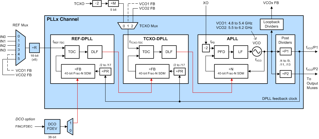
LMK05028 lmk05028-pll-core-3loop-fbd.gifFigure 20. 3-Loop Mode with DCO Option