ZHCSHN9A February 2018 – April 2018 LMK05028
PRODUCTION DATA.
- 1 特性
- 2 应用
- 3 说明
- 4 修订历史记录
- 5 说明 (续)
- 6 Pin Configuration and Functions
- 7 Specifications
- 8 Parameter Measurement Information
-
9 Detailed Description
- 9.1 Overview
- 9.2 Functional Block Diagrams
- 9.3
Feature Description
- 9.3.1 Oscillator Input (XO_P/N)
- 9.3.2 TCXO/OCXO Input (TCXO_IN)
- 9.3.3 Reference Inputs (INx_P/N)
- 9.3.4 Clock Input Interfacing and Termination
- 9.3.5 Reference Input Mux Selection
- 9.3.6 Hitless Switching
- 9.3.7 Gapped Clock Support on Reference Inputs
- 9.3.8 Input Clock and PLL Monitoring, Status, and Interrupts
- 9.3.9
PLL Channels
- 9.3.9.1 PLL Frequency Relationships
- 9.3.9.2 Analog PLL (APLL)
- 9.3.9.3 APLL XO Doubler
- 9.3.9.4 APLL Phase Frequency Detector (PFD) and Charge Pump
- 9.3.9.5 APLL Loop Filter
- 9.3.9.6 APLL Voltage Controlled Oscillator (VCO)
- 9.3.9.7 APLL VCO Post-Dividers (P1, P2)
- 9.3.9.8 APLL Fractional N Divider (N) With SDM
- 9.3.9.9 REF-DPLL Reference Divider (R)
- 9.3.9.10 TCXO/OCXO Input Doubler and M Divider
- 9.3.9.11 TCXO Mux
- 9.3.9.12 REF-DPLL and TCXO-DPLL Time-to-Digital Converter (TDC)
- 9.3.9.13 REF-DPLL and TCXO-DPLL Loop Filter
- 9.3.9.14 REF-DPLL and TCXO-DPLL Feedback Dividers
- 9.3.10 Output Clock Distribution
- 9.3.11 Output Channel Muxes
- 9.3.12 Output Dividers
- 9.3.13 Clock Outputs (OUTx_P/N)
- 9.3.14 Glitchless Output Clock Start-Up
- 9.3.15 Clock Output Interfacing and Termination
- 9.3.16 Output Synchronization (SYNC)
- 9.3.17 Zero-Delay Mode (ZDM) Configuration
- 9.3.18 PLL Cascading With Internal VCO Loopback
- 9.4 Device Functional Modes
- 9.5 Programming
- 9.6 Register Maps
- 10Application and Implementation
- 11Power Supply Recommendations
- 12Layout
- 13器件和文档支持
- 14机械、封装和可订购信息
9.2.4 2-Loop TCXO-DPLL Mode
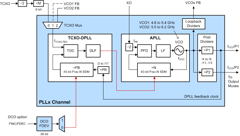
The principle of operation for 2-loop TCXO-DPLL mode is similar to 3-loop mode except the REF-DPLL stage is bypassed. After power-on reset and initialization, the APLL locks the VCO to the external XO input clock and operates in free-run mode. Once the external TCXO/OCXO input clock is detected, the TCXO-DPLL begins lock acquisition. The TCXO TDC compares the phase of the TCXO/OCXO clock and the TCXO FB divider clock (from the VCO) and generates a digital correction word corresponding to the phase error. The correction word is filtered by the TCXO DLF, and its output controls the APLL N divider SDM to pull the VCO frequency until it is locked to the TCXO/OCXO clock.
If DCO mode is enabled on the TCXO-DPLL, a frequency deviation step value (FDEV) can be programmed and used to adjust (increment or decrement) the TCXO FB divider SDM, where the frequency adjustment effectively propagates through the two nested loops to the VCO output.
In 2-loop mode, the TCXO-DPLL loop bandwidth (BWTCXO-DPLL) must less fTCXO/50 and less than the maximum bandwidth of 4 kHz.
When operating in 2-loop mode and the TCXO input is lost, the PLL channel will operate similar to 1-loop APLL only mode.
 Figure 23. 2-Loop TCXO-DPLL Mode With DCO Option