ZHCSHN9A February   2018  – April 2018 LMK05028

PRODUCTION DATA.  

  1. 特性
  2. 应用
  3. 说明
    1.     Device Images
      1.      简化方框图
  4. 修订历史记录
  5. 说明 (续)
  6. Pin Configuration and Functions
    1.     Pin Functions
    2. 6.1 Device Start-Up Modes
  7. Specifications
    1. 7.1 Absolute Maximum Ratings
    2. 7.2 ESD Ratings
    3. 7.3 Recommended Operating Conditions
    4. 7.4 Thermal Information
    5. 7.5 Electrical Characteristics
    6. 7.6 Timing Diagrams
    7. 7.7 Typical Characteristics
  8. Parameter Measurement Information
    1. 8.1 Output Clock Test Configurations
  9. Detailed Description
    1. 9.1 Overview
      1. 9.1.1 ITU-T G.8262 (SyncE) Standards Compliance
    2. 9.2 Functional Block Diagrams
      1. 9.2.1 PLL Architecture Overview
      2. 9.2.2 3-Loop Mode
        1. 9.2.2.1 PLL Output Clock Phase Noise Analysis in 3-Loop Mode
      3. 9.2.3 2-Loop REF-DPLL Mode
      4. 9.2.4 2-Loop TCXO-DPLL Mode
      5. 9.2.5 PLL Configurations for Common Applications
    3. 9.3 Feature Description
      1. 9.3.1  Oscillator Input (XO_P/N)
      2. 9.3.2  TCXO/OCXO Input (TCXO_IN)
      3. 9.3.3  Reference Inputs (INx_P/N)
      4. 9.3.4  Clock Input Interfacing and Termination
      5. 9.3.5  Reference Input Mux Selection
        1. 9.3.5.1 Automatic Input Selection
        2. 9.3.5.2 Manual Input Selection
      6. 9.3.6  Hitless Switching
      7. 9.3.7  Gapped Clock Support on Reference Inputs
      8. 9.3.8  Input Clock and PLL Monitoring, Status, and Interrupts
        1. 9.3.8.1 XO Input Monitoring
        2. 9.3.8.2 TCXO Input Monitoring
        3. 9.3.8.3 Reference Input Monitoring
          1. 9.3.8.3.1 Reference Validation Timer
          2. 9.3.8.3.2 Amplitude Monitor
          3. 9.3.8.3.3 Missing Pulse Monitor (Late Detect)
          4. 9.3.8.3.4 Runt Pulse Monitor (Early Detect)
          5. 9.3.8.3.5 Frequency Monitoring
          6. 9.3.8.3.6 Phase Valid Monitor for 1-PPS Inputs
        4. 9.3.8.4 PLL Lock Detectors
        5. 9.3.8.5 Tuning Word History
        6. 9.3.8.6 Status Outputs
        7. 9.3.8.7 Interrupt
      9. 9.3.9  PLL Channels
        1. 9.3.9.1  PLL Frequency Relationships
        2. 9.3.9.2  Analog PLL (APLL)
        3. 9.3.9.3  APLL XO Doubler
        4. 9.3.9.4  APLL Phase Frequency Detector (PFD) and Charge Pump
        5. 9.3.9.5  APLL Loop Filter
        6. 9.3.9.6  APLL Voltage Controlled Oscillator (VCO)
          1. 9.3.9.6.1 VCO Calibration
        7. 9.3.9.7  APLL VCO Post-Dividers (P1, P2)
        8. 9.3.9.8  APLL Fractional N Divider (N) With SDM
        9. 9.3.9.9  REF-DPLL Reference Divider (R)
        10. 9.3.9.10 TCXO/OCXO Input Doubler and M Divider
        11. 9.3.9.11 TCXO Mux
        12. 9.3.9.12 REF-DPLL and TCXO-DPLL Time-to-Digital Converter (TDC)
        13. 9.3.9.13 REF-DPLL and TCXO-DPLL Loop Filter
        14. 9.3.9.14 REF-DPLL and TCXO-DPLL Feedback Dividers
      10. 9.3.10 Output Clock Distribution
      11. 9.3.11 Output Channel Muxes
        1. 9.3.11.1 TCXO/Ref Bypass Mux
      12. 9.3.12 Output Dividers
      13. 9.3.13 Clock Outputs (OUTx_P/N)
        1. 9.3.13.1 AC-Differential Output (AC-DIFF)
        2. 9.3.13.2 HCSL Output
        3. 9.3.13.3 LVCMOS Output (1.8 V, 2.5 V)
        4. 9.3.13.4 Output Auto-Mute During LOL or LOS
      14. 9.3.14 Glitchless Output Clock Start-Up
      15. 9.3.15 Clock Output Interfacing and Termination
      16. 9.3.16 Output Synchronization (SYNC)
      17. 9.3.17 Zero-Delay Mode (ZDM) Configuration
      18. 9.3.18 PLL Cascading With Internal VCO Loopback
    4. 9.4 Device Functional Modes
      1. 9.4.1 Device Start-Up Modes
        1. 9.4.1.1 EEPROM Mode
        2. 9.4.1.2 ROM Mode
      2. 9.4.2 PLL Operating Modes
        1. 9.4.2.1 Free-Run Mode
        2. 9.4.2.2 Lock Acquisition
        3. 9.4.2.3 Locked Mode
        4. 9.4.2.4 Holdover Mode
      3. 9.4.3 PLL Start-Up Sequence
      4. 9.4.4 Digitally-Controlled Oscillator (DCO) Mode
        1. 9.4.4.1 DCO Frequency Step Size
        2. 9.4.4.2 DCO Direct-Write Mode
      5. 9.4.5 Zero-Delay Mode (ZDM)
      6. 9.4.6 Cascaded PLL Operation
    5. 9.5 Programming
      1. 9.5.1 Interface and Control
      2. 9.5.2 I2C Serial Interface
        1. 9.5.2.1 I2C Block Register Transfers
      3. 9.5.3 SPI Serial Interface
        1. 9.5.3.1 SPI Block Register Transfer
      4. 9.5.4 Register Map Generation
      5. 9.5.5 General Register Programming Sequence
      6. 9.5.6 EEPROM Programming Flow
        1. 9.5.6.1 EEPROM Programming Using Register Commit (Method #1)
          1. 9.5.6.1.1 Write SRAM Using Register Commit
          2. 9.5.6.1.2 Program EEPROM
        2. 9.5.6.2 EEPROM Programming Using Direct SRAM Writes (Method #2)
          1. 9.5.6.2.1 Write SRAM Using Direct Writes
      7. 9.5.7 Read SRAM
      8. 9.5.8 Read EEPROM
      9. 9.5.9 EEPROM Start-Up Mode Default Configuration
    6. 9.6 Register Maps
  10. 10Application and Implementation
    1. 10.1 Application Information
      1. 10.1.1 Device Start-Up Sequence
      2. 10.1.2 Power Down (PDN) Pin
      3. 10.1.3 Power Rail Sequencing, Power Supply Ramp Rate, and Mixing Supply Domains
        1. 10.1.3.1 Mixing Supplies
        2. 10.1.3.2 Power-On Reset (POR) Circuit
        3. 10.1.3.3 Powering Up From a Single-Supply Rail
        4. 10.1.3.4 Power Up From Split-Supply Rails
        5. 10.1.3.5 Non-Monotonic or Slow Power-Up Supply Ramp
      4. 10.1.4 Slow or Delayed XO Start-Up
    2. 10.2 Typical Application
      1. 10.2.1 Design Requirements
      2. 10.2.2 Detailed Design Procedure
      3. 10.2.3 Application Curves
    3. 10.3 Do's and Don'ts
  11. 11Power Supply Recommendations
    1. 11.1 Power Supply Bypassing
  12. 12Layout
    1. 12.1 Layout Guidelines
    2. 12.2 Layout Example
    3. 12.3 Thermal Reliability
  13. 13器件和文档支持
    1. 13.1 器件支持
      1. 13.1.1 时钟架构
      2. 13.1.2 TICS Pro
    2. 13.2 文档支持
      1. 13.2.1 相关文档
    3. 13.3 接收文档更新通知
    4. 13.4 社区资源
    5. 13.5 商标
    6. 13.6 静电放电警告
    7. 13.7 术语表
  14. 14机械、封装和可订购信息

Manual Input Selection

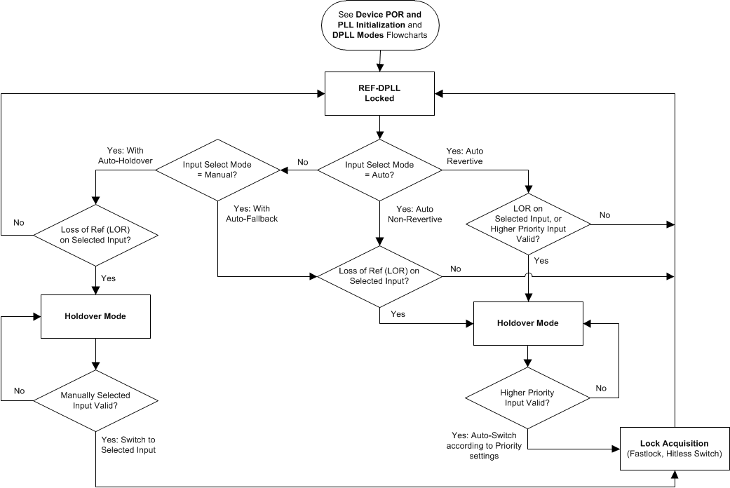
There are two manual input selection modes that can be set by a register: Manual with Auto-Fallback and Manual with Auto-Holdover. In either manual mode, the input selection can be done through register control (Table 6) or hardware pin control (Table 7).

  • Manual with Auto-Fallback: In this mode, the manually selected reference is the active reference until it becomes invalid. If the reference becomes invalid, the DPLL will automatically fallback to the highest priority input that is valid or qualified. If no prioritized inputs are valid, the DPLL will enter holdover mode (if tuning word history is valid) or free-run mode. The DPLL will exit holdover mode when the selected input becomes valid.
  • Manual with Auto-Holdover: In this mode, the manually selected reference is the active reference until it becomes invalid. If the reference becomes invalid, the DPLL will automatically enter holdover mode (if tuning word history is valid) or free-run mode. The DPLL will exit holdover mode when the selected input becomes valid.

Table 6. Manual Input Selection by Register Bits

DPLLx_REF_MAN_REG_SEL[2:0] BITS DPLLx_REF_MAN_SEL BIT SELECTED INPUT
000b 0 IN0
001b 0 IN1
010b 0 IN2
011b 0 IN3
100b 0 VCO1 Loopback to DPLL2
101b 0 VCO2 Loopback to DPLL1

Table 7. Manual Input Selection by Hardware Pins

INSELx_[1:0] PINS DPLLx_REF_MAN_SEL BIT SELECTED INPUT
00b 1 IN0
01b 1 IN1
10b 1 IN2
11b 1 IN3

The reference input selection flowchart is shown in Figure 35.
LMK05028 lmk05028-input-selection-flowchart.gifFigure 35. Reference Input Selection Flowchart