ZHCSHO1D November   2018  – January 2019 LMG1210

PRODUCTION DATA.  

  1. 特性
  2. 应用
  3. 说明
    1.     Device Images
      1.      简化的典型应用
  4. 修订历史记录
  5. Pin Configuration and Functions
    1.     Pin Functions
  6. Specifications
    1. 6.1 Absolute Maximum Ratings
    2. 6.2 ESD Ratings
    3. 6.3 Recommended Operating Conditions
    4. 6.4 Thermal Information
    5. 6.5 Electrical Characteristics
    6. 6.6 Switching Characteristics
    7. 6.7 Typical Characteristics
    8. 6.8 Timing Diagrams
  7. Detailed Description
    1. 7.1 Overview
    2. 7.2 Functional Block Diagram
    3. 7.3 Feature Description
      1. 7.3.1 Bootstrap Diode Operation
      2. 7.3.2 LDO Operation
      3. 7.3.3 Dead Time Selection
      4. 7.3.4 Overtemperature Protection
      5. 7.3.5 High-Performance Level Shifter
      6. 7.3.6 Negative HS Voltage Handling
    4. 7.4 Device Functional Modes
  8. Application and Implementation
    1. 8.1 Application Information
    2. 8.2 Typical Application
      1. 8.2.1 Design Requirements
      2. 8.2.2 Detailed Design Procedure
        1. 8.2.2.1 Bypass Capacitor
        2. 8.2.2.2 Bootstrap Diode Selection
        3. 8.2.2.3 Handling Ground Bounce
        4. 8.2.2.4 Independent Input Mode
        5. 8.2.2.5 Computing Power Dissipation
      3. 8.2.3 Application Curves
    3. 8.3 Do's and Don'ts
  9. Power Supply Recommendations
  10. 10Layout
    1. 10.1 Layout Guidelines
    2. 10.2 Layout Example
  11. 11器件和文档支持
    1. 11.1 文档支持
      1. 11.1.1 相关文档
    2. 11.2 接收文档更新通知
    3. 11.3 社区资源
    4. 11.4 商标
    5. 11.5 静电放电警告
    6. 11.6 术语表
  12. 12机械、封装和可订购信息

Typical Characteristics

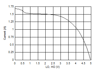
LMG1210 D001_source_current.gifFigure 1. Peak Source Current vs Output Voltage
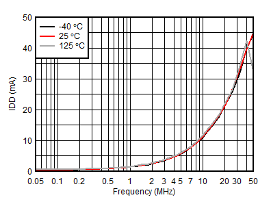
LMG1210 D003_IDDO_freq.gifFigure 3. IDD vs Frequency, Unloaded
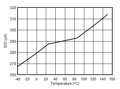
LMG1210 D005_Temp_IDDQ.gifFigure 5. IDD vs Temperature
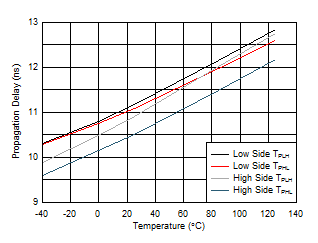
LMG1210 D007_prop_temp.gifFigure 7. Propagation Delay vs Temperature
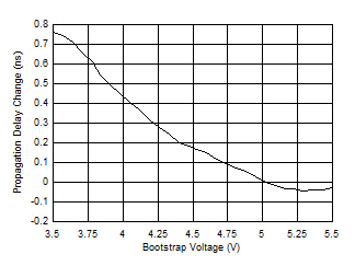
LMG1210 D009_Delay_HB_HS_voltage.gifFigure 9. Propagation Delay Change vs Bootstrap voltage
LMG1210 D011_OutputCurrent_Temp.gifFigure 11. LO and HO Output Current vs Temperature
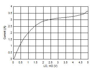
LMG1210 D002_sink_current.gifFigure 2. Peak Sink Current vs Output Voltage
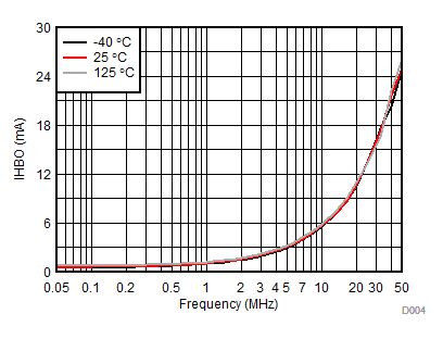
LMG1210 D004_IHBO_freq.gifFigure 4. IHBO vs Frequency, Unloaded
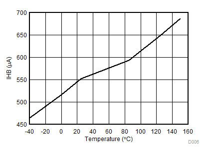
LMG1210 D006_Temp_IHBQ.gifFigure 6. IHB vs Temperature
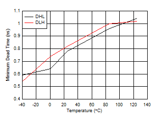
LMG1210 D008_min_dead_temp.gifFigure 8. Minimum Dead Time vs Temperature
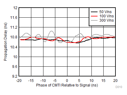
LMG1210 D010_Prop_delay_CMTI_2.gifFigure 10. Propagation Delay vs relative phase of CMTI Phase
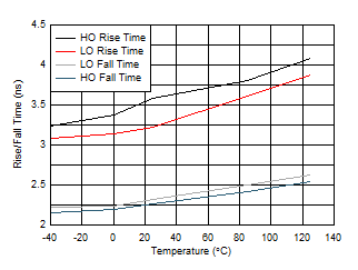
LMG1210 D012_rise_fall_temp.gifFigure 12. 1 nF Loaded Rise and Fall Time vs Temperature