ZHCSHO2G June 2010 – February 2018 TPS65251
PRODUCTION DATA.
- 1 特性
- 2 应用
- 3 说明
- 4 修订历史记录
- 5 说明 (续)
- 6 Pin Configuration and Functions
- 7 Specifications
-
8 Detailed Description
- 8.1 Overview
- 8.2 Functional Block Diagram
- 8.3
Feature Description
- 8.3.1 Adjustable Switching Frequency
- 8.3.2 Synchronization
- 8.3.3 Out-of-Phase Operation
- 8.3.4 Delayed Start-Up
- 8.3.5 Soft-Start Time
- 8.3.6 Adjusting the Output Voltage
- 8.3.7 Input Capacitor
- 8.3.8 Bootstrap Capacitor
- 8.3.9 Error Amplifier
- 8.3.10 Loop Compensation
- 8.3.11 Slope Compensation
- 8.3.12 Powergood
- 8.3.13 Current Limit Protection
- 8.3.14 Overvoltage Transient Protection
- 8.3.15 Thermal Shutdown
- 8.4 Device Functional Modes
-
9 Application and Implementation
- 9.1 Application Information
- 9.2
Typical Application
- 9.2.1 Design Requirements
- 9.2.2
Detailed Design Procedure
- 9.2.2.1 Loop Compensation Circuit
- 9.2.2.2 Selecting the Switching Frequency
- 9.2.2.3 Output Inductor Selection
- 9.2.2.4 Output Capacitor
- 9.2.2.5 Input Capacitor
- 9.2.2.6 Soft-Start Capacitor
- 9.2.2.7 Bootstrap Capacitor Selection
- 9.2.2.8 Adjustable Current Limiting Resistor Selection
- 9.2.2.9 Output Voltage and Feedback Resistors Selection
- 9.2.2.10 Compensation
- 9.2.2.11 3.3-V and 6.5-V LDO Regulators
- 9.2.3 Application Curves
- 10Power Supply Recommendations
- 11Layout
- 12器件和文档支持
- 13机械、封装和可订购信息
11.3 Power Dissipation
The total power dissipation inside TPS65251 should not to exceed the maximum allowable junction temperature of 125°C. The maximum allowable power dissipation is a function of the thermal resistance of the package (RJA) and ambient temperature.
To calculate the temperature inside the device under continuous loading use the following procedure.
- Define the set voltage for each converter.
- Define the continuous loading on each converter. Make sure do not exceed the converter maximum loading.
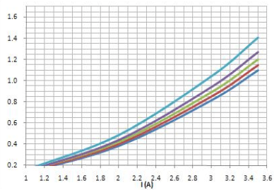
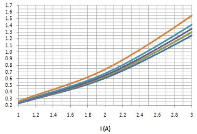
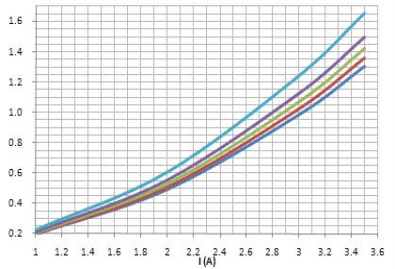
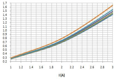
- Determine from the graphs below the expected losses (Y axis) in watts per converter inside the device. The losses depend on the input supply, the selected switching frequency, the output voltage and the converter chosen.
- To calculate the maximum temperature inside the IC use the following formula:
- TA is the ambient temperature
- PDIS is the sum of losses in all converters
- θJA is the junction to ambient thermal impedance of the device and it is heavily dependant on board layout
Equation 27. 

where

| VO (from top to bottom) = 5 V , 3.3 V, 2.5 V, 1.8 V, 1.2 V | ||
VIN = 12 V, ƒSW = 500 kHz

| VO (from top to bottom) = 5 V , 3.3 V, 2.5 V, 1.8 V, 1.2 V | ||
VIN = 12 V, ƒSW = 500 kHz

| VO (from top to bottom) = 5 V , 3.3 V, 2.5 V, 1.8 V, 1.2 V | ||
VIN = 12 V, ƒSW = 1.1 MHz

| VO (from top to bottom) = 5 V , 3.3 V, 2.5 V, 1.8 V, 1.2 V | ||
VIN = 12 V, ƒSW = 1.1 MHz