ZHCSHP3 February 2018 DAC8771
PRODUCTION DATA.
- 1 特性
- 2 应用
- 3 说明
- 4 修订历史记录
- 5 Device Comparison Table
- 6 Pin Configuration and Functions
- 7 Specifications
-
8 Detailed Description
- 8.1 Overview
- 8.2 Functional Block Diagram
- 8.3
Feature Description
- 8.3.1 Current Output Stage
- 8.3.2 Voltage Output Stage
- 8.3.3 Buck-Boost Converter
- 8.3.4 Analog Power Supply
- 8.3.5 Digital Power Supply
- 8.3.6 Internal Reference
- 8.3.7 Power-On-Reset
- 8.3.8 ALARM Pin
- 8.3.9 Power GOOD bit
- 8.3.10 Status Register
- 8.3.11 Status Mask
- 8.3.12 Alarm Action
- 8.3.13 Watchdog Timer
- 8.3.14 Programmable Slew Rate
- 8.3.15 HART Interface
- 8.4 Device Functional Modes
- 8.5
Register Maps
- 8.5.1
Register Maps
- 8.5.1.1 DAC8771 Commands
- 8.5.1.2
Register Maps and Bit Functions
- 8.5.1.2.1 No Operation Register (address = 0x00) [reset = 0x0000]
- 8.5.1.2.2 Reset Register (address = 0x01) [reset = 0x0000]
- 8.5.1.2.3 Reset Config Register (address = 0x02) [reset = 0x0000]
- 8.5.1.2.4 Select DAC Register (address = 0x03) [reset = 0x0000]
- 8.5.1.2.5 Configuration DAC Register (address = 0x04) [reset = 0x0000]
- 8.5.1.2.6 DAC Data Register (address = 0x05) [reset = 0x0000]
- 8.5.1.2.7 Select Buck-Boost Converter Register (address = 0x06) [reset = 0x0000]
- 8.5.1.2.8 Configuration Buck-Boost Register (address = 0x07) [reset = 0x0000]
- 8.5.1.2.9 DAC Channel Calibration Enable Register (address = 0x08) [reset = 0x0000]
- 8.5.1.2.10 DAC Channel Gain Calibration Register (address = 0x09) [reset = 0x0000]
- 8.5.1.2.11 DAC Channel Offset Calibration Register (address = 0x0A) [reset = 0x0000]
- 8.5.1.2.12 Status Register (address = 0x0B) [reset = 0x1000]
- 8.5.1.2.13 Status Mask Register (address = 0x0C) [reset = 0x0000]
- 8.5.1.2.14 Alarm Action Register (address = 0x0D) [reset = 0x0000]
- 8.5.1.2.15 User Alarm Code Register (address = 0x0E) [reset = 0x0000]
- 8.5.1.2.16 Reserved Register (address = 0x0F) [reset = N/A]
- 8.5.1.2.17 Write Watchdog Timer Register (address = 0x10) [reset = 0x0000]
- 8.5.1.2.18 Reserved Register (address 0x12 - 0xFF) [reset = N/A]
- 8.5.1
Register Maps
- 9 Application and Implementation
- 10Power Supply Recommendations
- 11Layout
- 12器件和文档支持
- 13机械、封装和可订购信息
9.1.4 Protection for Industrial Transients
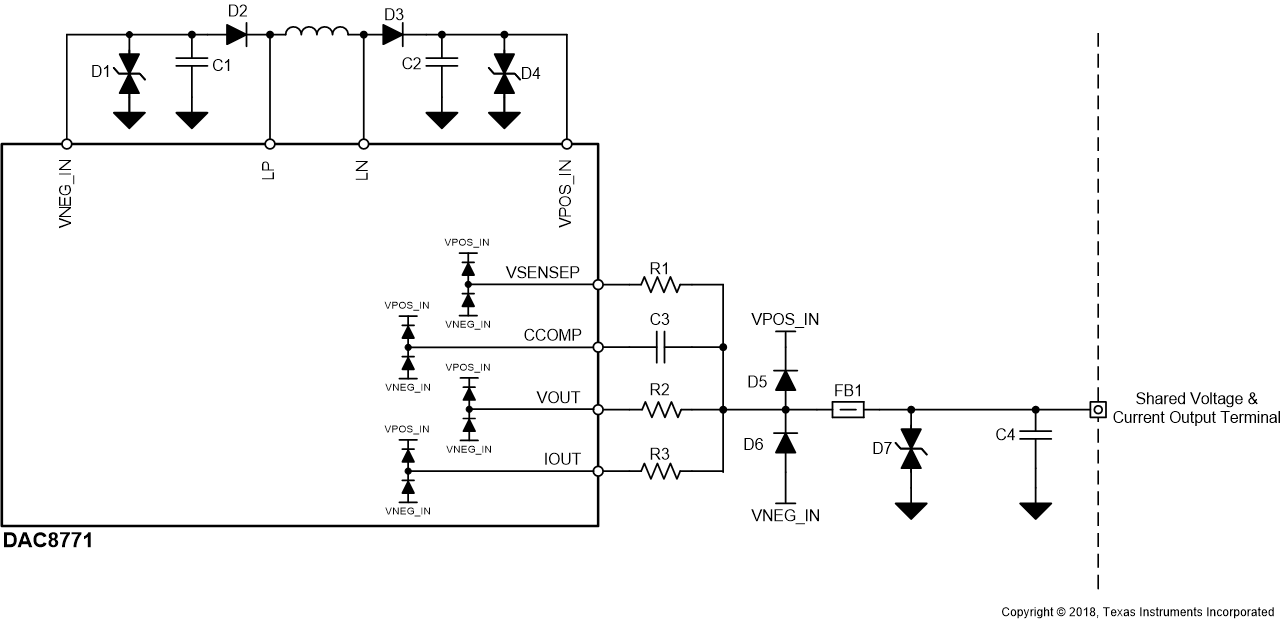
In order to successfully protect the DAC8771, or any integrated circuit, against industrial transient testing the internal structures and how they may behave when exposed to said signals must be understood. Figure 124 depicts a simplified representation of internal structures present on the device output pins which are represented as a pair of clamp-to-rail diodes connected to the VPOS_IN and VNEG_IN supply rails
 Figure 124. Simplified Block Diagram of Internal Structures and External Protection
When these internal structures are exposed to industrial transient testing, without the external protection components, the diode structures will become forward biased and conduct current. If the conducted current is too large, which is often true for high-voltage industrial transient tests, the structures will become permanently damaged and impact device functionality.
Both attenuation and diversion strategies are implemented to protect the internal structures as well as the device itself. Attenuation is realized by capacitor C4 which forms an R/C low-pass filter when interacting with the source impedance of the transient generator, ferrite bead FB1 also helps attenuate high-frequency current, along with both AC and DC current limiters realized by series pass elements R1, R2, and R3. Diversion is achieved by transient voltage suppressor (TVS) diode D7 and clamp-to-rail diodes D5 and D6. The combined effects of both strategies effectively limit the current flowing into the device and through the internal diode structures such that the device is not damaged and remains functional.
It is important to also include TVS diodes D1 and D4 at the VPOS_IN and VNEG_IN nodes in order to provide a discharge path for the energy that is going to be sent to these nodes through diodes D5, D6, and the internal diode structures. Without these diodes when current is diverted to these nodes, the DC/DC converter storage capacitors C1 and C2 will charge, and slowly increasing the voltage at these nodes.