ZHCSHP3 February   2018 DAC8771

PRODUCTION DATA.  

  1. 特性
  2. 应用
  3. 说明
    1.     Device Images
      1.      DAC8771 框图
  4. 修订历史记录
  5. Device Comparison Table
  6. Pin Configuration and Functions
    1.     Pin Functions
  7. Specifications
    1. 7.1 Absolute Maximum Ratings
    2. 7.2 ESD Ratings
    3. 7.3 Recommended Operating Conditions
    4. 7.4 Thermal Information
    5. 7.5 Electrical Characteristics
    6. 7.6 Timing Requirements: Write and Readback Mode
    7. 7.7 Typical Characteristics
  8. Detailed Description
    1. 8.1 Overview
    2. 8.2 Functional Block Diagram
    3. 8.3 Feature Description
      1. 8.3.1  Current Output Stage
      2. 8.3.2  Voltage Output Stage
      3. 8.3.3  Buck-Boost Converter
        1. 8.3.3.1 Buck-Boost Converter Outputs
        2. 8.3.3.2 Selecting and Enabling Buck-Boost Converter
        3. 8.3.3.3 Configurable Clamp Feature and Current Output Settling Time
          1. 8.3.3.3.1 Default Mode - CCLP[1:0] = "00"
          2. 8.3.3.3.2 Fixed Clamp Mode - CCLP[1:0] = "01"
          3. 8.3.3.3.3 Auto Learn Mode - CCLP[1:0] = "10"
          4. 8.3.3.3.4 High Side Clamp (HSCLMP)
      4. 8.3.4  Analog Power Supply
      5. 8.3.5  Digital Power Supply
      6. 8.3.6  Internal Reference
      7. 8.3.7  Power-On-Reset
      8. 8.3.8  ALARM Pin
      9. 8.3.9  Power GOOD bit
      10. 8.3.10 Status Register
      11. 8.3.11 Status Mask
      12. 8.3.12 Alarm Action
      13. 8.3.13 Watchdog Timer
      14. 8.3.14 Programmable Slew Rate
      15. 8.3.15 HART Interface
    4. 8.4 Device Functional Modes
      1. 8.4.1 Serial Peripheral Interface (SPI)
        1. 8.4.1.1 Stand-Alone Operation
        2. 8.4.1.2 Daisy-Chain Operation
      2. 8.4.2 SPI Shift Register
      3. 8.4.3 Write Operation
      4. 8.4.4 Read Operation
      5. 8.4.5 Updating the DAC Outputs and LDAC Pin
        1. 8.4.5.1 Asynchronous Mode
        2. 8.4.5.2 Synchronous Mode
      6. 8.4.6 Hardware RESET Pin
      7. 8.4.7 Hardware CLR Pin
      8. 8.4.8 Frame Error Checking
      9. 8.4.9 DAC Data Calibration
        1. 8.4.9.1 DAC Data Gain and Offset Calibration Registers
    5. 8.5 Register Maps
      1. 8.5.1 Register Maps
        1. 8.5.1.1 DAC8771 Commands
        2. 8.5.1.2 Register Maps and Bit Functions
          1. 8.5.1.2.1  No Operation Register (address = 0x00) [reset = 0x0000]
            1. Table 6. No Operation Field Descriptions
          2. 8.5.1.2.2  Reset Register (address = 0x01) [reset = 0x0000]
            1. Table 7. Reset Register Field Descriptions
          3. 8.5.1.2.3  Reset Config Register (address = 0x02) [reset = 0x0000]
            1. Table 8. Reset Config Register Field Descriptions
          4. 8.5.1.2.4  Select DAC Register (address = 0x03) [reset = 0x0000]
            1. Table 9. Select DAC Register Field Descriptions
          5. 8.5.1.2.5  Configuration DAC Register (address = 0x04) [reset = 0x0000]
            1. Table 10. Configuration DAC Register Field Descriptions
          6. 8.5.1.2.6  DAC Data Register (address = 0x05) [reset = 0x0000]
            1. Table 11. DAC Data Register Field Descriptions
          7. 8.5.1.2.7  Select Buck-Boost Converter Register (address = 0x06) [reset = 0x0000]
            1. Table 12. Select Buck-Boost Converter Register Field Descriptions
          8. 8.5.1.2.8  Configuration Buck-Boost Register (address = 0x07) [reset = 0x0000]
            1. Table 13. Configuration Buck-Boost Register Field Descriptions
          9. 8.5.1.2.9  DAC Channel Calibration Enable Register (address = 0x08) [reset = 0x0000]
            1. Table 14. DAC Channel Calibration Enable Register Field Descriptions
          10. 8.5.1.2.10 DAC Channel Gain Calibration Register (address = 0x09) [reset = 0x0000]
            1. Table 15. DAC Channel Gain Calibration Register Field Descriptions
          11. 8.5.1.2.11 DAC Channel Offset Calibration Register (address = 0x0A) [reset = 0x0000]
            1. Table 16. DAC Channel Offset Calibration Register Field Descriptions
          12. 8.5.1.2.12 Status Register (address = 0x0B) [reset = 0x1000]
            1. Table 17. Status Register Field Descriptions
          13. 8.5.1.2.13 Status Mask Register (address = 0x0C) [reset = 0x0000]
            1. Table 18. Status Mask Register Field Descriptions
          14. 8.5.1.2.14 Alarm Action Register (address = 0x0D) [reset = 0x0000]
            1. Table 19. Alarm Action Register Field Descriptions
          15. 8.5.1.2.15 User Alarm Code Register (address = 0x0E) [reset = 0x0000]
            1. Table 20. User Alarm Code Register Field Descriptions
          16. 8.5.1.2.16 Reserved Register (address = 0x0F) [reset = N/A]
            1. Table 21. Reserved Register Field Descriptions
          17. 8.5.1.2.17 Write Watchdog Timer Register (address = 0x10) [reset = 0x0000]
            1. Table 22. Write Watchdog Timer Register Field Descriptions
          18. 8.5.1.2.18 Reserved Register (address 0x12 - 0xFF) [reset = N/A]
            1. Table 23. Reserved Register Field Descriptions
  9. Application and Implementation
    1. 9.1 Application Information
      1. 9.1.1 Buck-Boost Converter External Component Selection
      2. 9.1.2 Voltage and Current Outputs on a Shared Terminal
      3. 9.1.3 Optimizing Current Output Settling Time with Auto-Learn Mode
      4. 9.1.4 Protection for Industrial Transients
      5. 9.1.5 Implementing HART with DAC8771
    2. 9.2 Typical Application
      1. 9.2.1 Single-Channel, Isolated, EMC and EMI Protected Analog Output Module with Adaptive Power Management
      2. 9.2.2 Design Requirements
      3. 9.2.3 Detailed Design Procedure
      4. 9.2.4 Application Curves
  10. 10Power Supply Recommendations
  11. 11Layout
    1. 11.1 Layout Guidelines
    2. 11.2 Layout Example
  12. 12器件和文档支持
    1. 12.1 器件支持
      1. 12.1.1 Third-Party Products Disclaimer
    2. 12.2 文档支持
      1. 12.2.1 相关文档
    3. 12.3 接收文档更新通知
    4. 12.4 社区资源
    5. 12.5 商标
    6. 12.6 静电放电警告
    7. 12.7 Glossary
  13. 13机械、封装和可订购信息

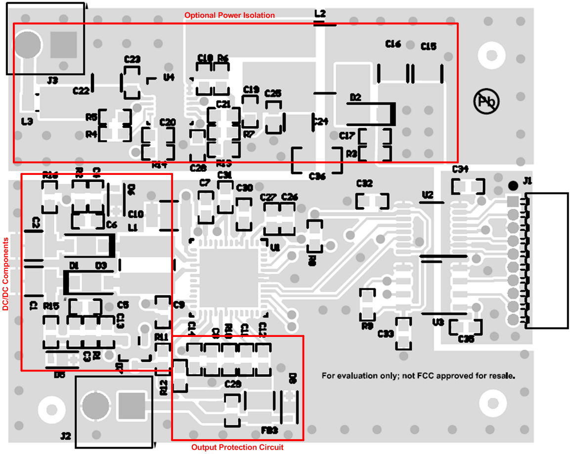
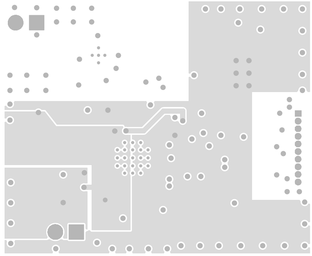
Layout Example

DAC8771 SLASEE2_PCBLayoutTopLayer.gifFigure 132. Application Example Layout
DAC8771 SLASEE2_PCBLayoutPowerLayers.gifFigure 133. Example Design Internal Copper Pours
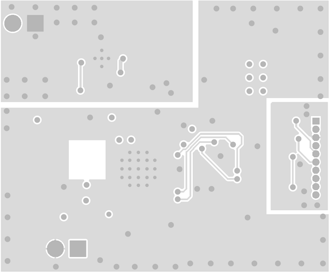
DAC8771 SLASEE2_PCBLayoutBottomLayer.gifFigure 134. Example Design Bottom Layer