ZHCSHQ3F August   2017  – November 2020 LMR33630

PRODUCTION DATA  

  1. 特性
  2. 应用
  3. 说明
  4. Revision History
  5. Device Comparison Table
  6. Pin Configuration and Functions
  7. Specifications
    1. 7.1 Absolute Maximum Ratings
    2. 7.2 ESD Ratings
    3. 7.3 Recommended Operating Conditions
    4. 7.4 Thermal Information
    5. 7.5 Electrical Characteristics
    6. 7.6 Timing Characteristics
    7. 7.7 System Characteristics
    8. 7.8 Typical Characteristics
  8. Detailed Description
    1. 8.1 Overview
    2. 8.2 Functional Block Diagram
    3. 8.3 Feature Description
      1. 8.3.1 Power-Good Flag Output
      2. 8.3.2 Enable and Start-up
      3. 8.3.3 Current Limit and Short Circuit
      4. 8.3.4 Undervoltage Lockout and Thermal Shutdown
    4. 8.4 Device Functional Modes
      1. 8.4.1 Auto Mode
      2. 8.4.2 Dropout
      3. 8.4.3 Minimum Switch On-Time
  9. Application and Implementation
    1. 9.1 Application Information
    2. 9.2 Typical Application
      1. 9.2.1 Design Requirements
      2. 9.2.2 Detailed Design Procedure
        1. 9.2.2.1  Custom Design With WEBENCH® Tools
        2. 9.2.2.2  Choosing the Switching Frequency
        3. 9.2.2.3  Setting the Output Voltage
        4. 9.2.2.4  Inductor Selection
        5. 9.2.2.5  Output Capacitor Selection
        6. 9.2.2.6  Input Capacitor Selection
        7. 9.2.2.7  CBOOT
        8. 9.2.2.8  VCC
        9. 9.2.2.9  CFF Selection
        10. 9.2.2.10 External UVLO
        11. 9.2.2.11 Maximum Ambient Temperature
      3. 9.2.3 Application Curves
    3. 9.3 What to Do and What Not to Do
  10. 10Layout
    1. 10.1 Layout Guidelines
      1. 10.1.1 Ground and Thermal Considerations
    2. 10.2 Layout Example
  11. 11Device and Documentation Support
    1. 11.1 Device Support
      1. 11.1.1 Development Support
        1. 11.1.1.1 Custom Design With WEBENCH® Tools
    2. 11.2 Documentation Support
      1. 11.2.1 Related Documentation
    3. 11.3 接收文档更新通知
    4. 11.4 支持资源
    5. 11.5 Trademarks
    6. 11.6 静电放电警告
    7. 11.7 术语表

Typical Characteristics

Unless otherwise specified the following conditions apply: TA = 25°C and VIN = 12 V
GUID-0FF9913D-895C-493A-9A2F-64627E033E96-low.png
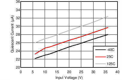
VFB = 1.2 V
Figure 7-1 Non-Switching Input Supply Current
GUID-DD5DA6AD-B5D9-41D8-A16D-080602611453-low.png
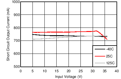
VOUT = 0 VƒS = 400 kHzSee Figure 9-31
Figure 7-3 Short-Circuit Output Current
GUID-333224F0-11DF-451B-937E-60736AC54D74-low.gif
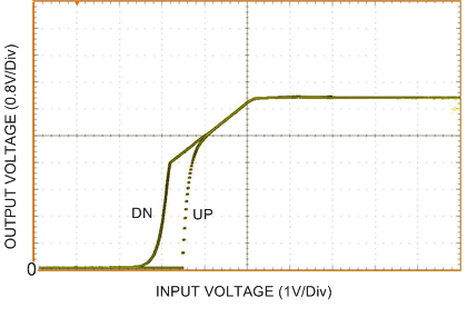
IOUT = 1 mASee Figure 9-31
Figure 7-5 UVLO Thresholds
GUID-B39617AE-BE8F-4E66-BD18-7CE800C1634E-low.png
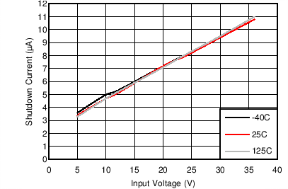
EN = 0 V
Figure 7-2 Shutdown Supply Current
GUID-2A765524-87CE-4354-8C79-0E21A7895681-low.png
 
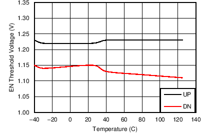
Figure 7-4 Precision Enable Thresholds
GUID-D01B571A-90BB-48DC-8BF6-58C27BC94455-low.png
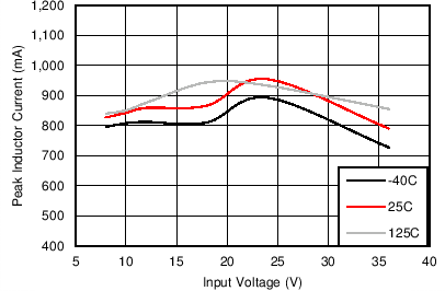
IOUT = 0 AVOUT = 5 VSee Figure 9-31
ƒSW = 400 kHz
Figure 7-6 IPEAK-MIN