ZHCSHR4F January 2009 – April 2018 DAC7568 , DAC8168 , DAC8568
PRODUCTION DATA.
- 1 特性
- 2 应用
- 3 说明
- 4 修订历史记录
- 5 Device Comparison Table
- 6 Pin Configuration and Functions
- 7 Specifications
-
8 Detailed Description
- 8.1 Functional Block Diagram
- 8.2
Feature Description
- 8.2.1 Digital-to-Analog Converter (DAC)
- 8.2.2 Resistor String
- 8.2.3 Output Amplifier
- 8.2.4 Internal Reference
- 8.2.5 Serial Interface
- 8.2.6 Input Shift Register
- 8.2.7 SYNC Interrupt
- 8.2.8 Power-on Reset to Zero Scale or Midscale
- 8.2.9 Clear Code Register and CLR Pin
- 8.2.10 Software Reset Function
- 8.2.11
Operating Examples: DAC7568/DAC8168/DAC8568
- Table 4. 1st: Write to Data Buffer A:
- Table 5. 2nd: Write to Data Buffer B:
- Table 6. 3rd: Write to Data Buffer G:
- Table 7. 4th: Write to Data Buffer H and Simultaneously Update all DACs:
- Table 8. 1st: Write to Data Buffer C and Load DAC C: DAC C Output Settles to Specified Value Upon Completion:
- Table 9. 2nd: Write to Data Buffer D and Load DAC D: DAC D Output Settles to Specified Value Upon Completion:
- Table 10. 3rd: Write to Data Buffer E and Load DAC E: DAC E Output Settles to Specified Value Upon Completion:
- Table 11. 4th: Write to Data Buffer F and Load DAC F: DAC F Output Settles to Specified Value Upon Completion:
- Table 12. 1st: Write Power-Down Command to DAC Channel A and DAC Channel B: DAC A and DAC B to 1kΩ.
- Table 13. 2nd: Write Power-Down Command to DAC Channel H: DAC H to 1kΩ.
- Table 14. 3rd: Write Power-Down Command to DAC Channel C and DAC Channel D: DAC C and DAC D to 100kΩ.
- Table 15. 4th: Write Power-Down Command to DAC Channel F: DAC F to 100kΩ.
- Table 16. 1st: Write Sequence for Enabling the DAC7568, DAC8168, and DAC8568 Internal Reference All the Time:
- Table 17. 2nd: Write Sequence to Power-Down All DACs to High-Impedance:
- Table 18. 1st: Write Sequence for Disabling the DAC7568, DAC8168, and DAC8568 Internal Reference All the Time (after this sequence, these devices require an external reference source to function):
- Table 19. 2nd: Write Sequence to Write Specified Data to All DACs:
- 8.3
Device Functional Modes
- 8.3.1
Enable/Disable Internal Reference
- 8.3.1.1 Static Mode
- 8.3.1.2
Flexible Mode
- Table 22. Write Sequence for Enabling Internal Reference (Flexible Mode) (Internal Reference Powered On—09080000h)
- Table 23. Write Sequence for Enabling Internal Reference (Flexible Mode) (Internal Reference Always Powered On—090A0000h)
- Table 24. Write Sequence for Disabling Internal Reference (Flexible Mode) (Internal Reference Always Powered Down—090C0000h)
- Table 25. Write Sequence for Switching from Flexible Mode to Static Mode for Internal Reference (Internal Reference Always Powered Down—09000000h)
- 8.3.2 LDAC Functionality
- 8.3.3 Power-Down Modes
- 8.3.1
Enable/Disable Internal Reference
-
9 Application and Implementation
- 9.1 Application Information
- 9.2
Typical Applications - Microprocessor Interfacing
- 9.2.1 DAC7568/DAC8168/DAC8568 to an 8051 Interface
- 9.2.2 DAC7568/DAC8168/DAC8568 to Microwire Interface
- 9.2.3 DAC7568/DAC8168/DAC8568 to 68HC11 Interface
- 10Layout
- 11器件和文档支持
- 12机械、封装和可订购信息
7.7 Typical Characteristics: DAC at AVDD = 2.7 V
Channel-specific information provided as examples. At TA = +25°C, internal reference used, and DAC output not loaded, all DAC codes in straight binary data format, unless otherwise noted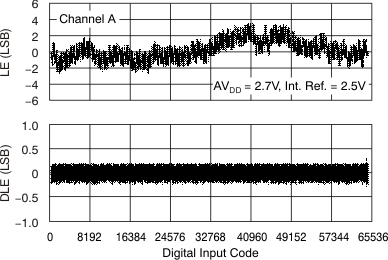 Figure 76. Linearity Error and Differential Linearity Error vs Digital Input Code (–40°C)
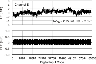 Figure 78. Linearity Error and Differential Linearity Error vs Digital Input Code (–40°C)
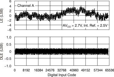 Figure 80. Linearity Error and Differential Linearity Error vs Digital Input Code (+25°C)
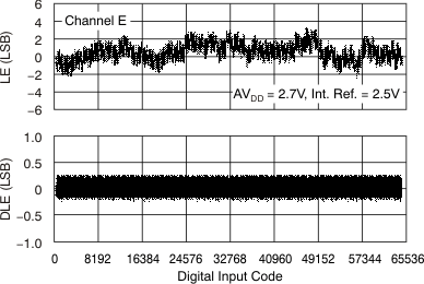 Figure 82. Linearity Error and Differential Linearity Error vs Digital Input Code (+25°C)
 Figure 84. Linearity Error and Differential Linearity Error vs Digital Input Code (+105°C)
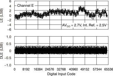 Figure 86. Linearity Error and Differential Linearity Error vs Digital Input Code (+105°C)
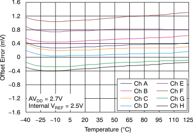 Figure 88. Offset Error vs Temperature
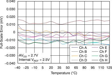 Figure 90. Full-Scale Error vs Temperature
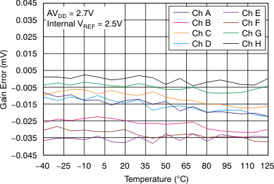 Figure 92. Gain Error vs Temperature
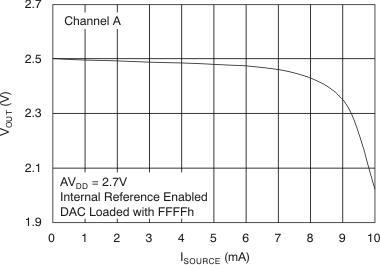 Figure 94. Source Current at Positive Rail (Grades A and B)
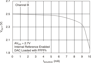 Figure 96. Source Current at Positive Rail (Grades A and B)
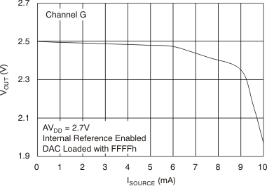 Figure 98. Source Current at Positive Rail (Grades A and B
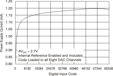 Figure 100. Power-Supply Current Vs Digital Input Code
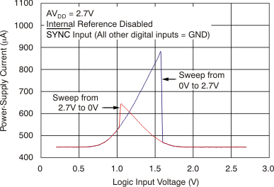 Figure 102. Power-Supply Current vs Logic Input Voltage
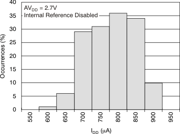 Figure 104. Power-Supply Current Histogram
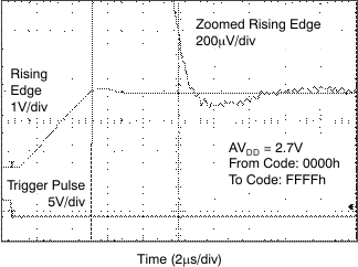 Figure 106. Full-Scale Settling Time: 2.7-V Rising Edge
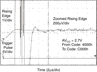 Figure 108. Half-Scale Settling Time: 2.7-V Rising Edge
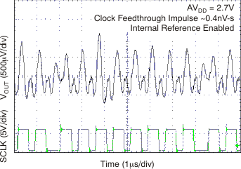 Figure 110. Clock Feedthrough 2.7 V, 2 Mhz, Midscale
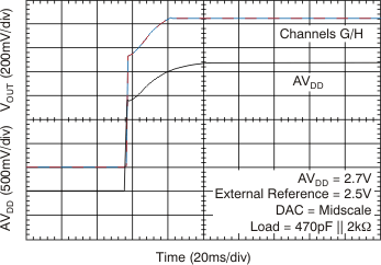 Figure 112. Power-On Glitch Reset to Midscale
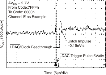 Figure 114. Glitch Energy: 2.7 V, 1-LSB Step, Rising Edge
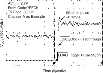 Figure 116. Glitch Energy: 2.7 V, 4-LSB Step, Rising Edge
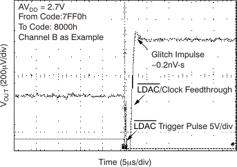 Figure 118. Glitch Energy: 2.7 V, 16-LSB Step, Rising Edge
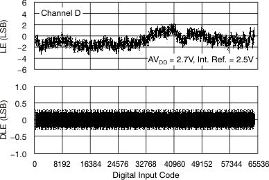 Figure 77. Linearity Error and Differential Linearity Error vs Digital Input Code (–40°C)
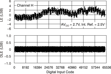 Figure 79. Linearity Error and Differential Linearity Error vs Digital Input Code (–40°C)
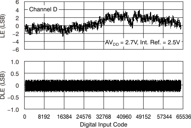 Figure 81. Linearity Error and Differential Linearity Error vs Digital Input Code (+25°C)
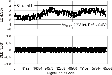 Figure 83. Linearity Error and Differential Linearity Error vs Digital Input Code (+25°C)
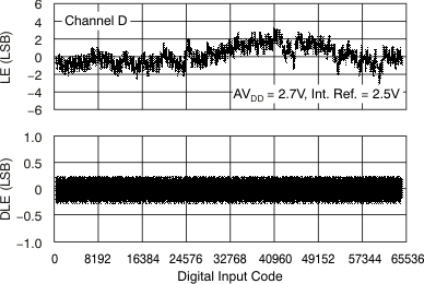 Figure 85. Linearity Error and Differential Linearity Error vs Digital Input Code (+105°C)
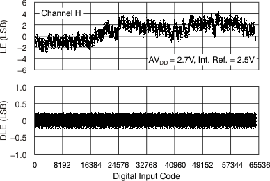 Figure 87. Linearity Error and Differential Linearity Error vs Digital Input Code (+105°C)
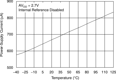 Figure 89. Power-Supply Current vs Temperature
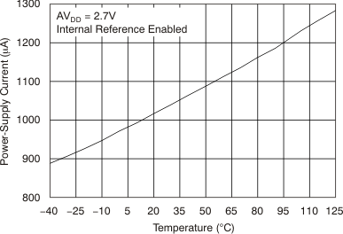 Figure 91. Power-Supply Current vs Temperature
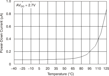 Figure 93. Power-Down Current vs Temperature
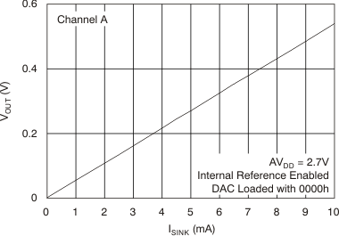 Figure 95. Sink Current at Negative Rail (All Grades)
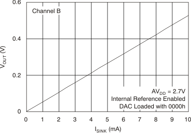 Figure 97. Sink Current at Negative Rail (All Grades)
 Figure 99. Sink Current at Negative Rail (All Grades)
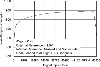 Figure 101. Power-Supply Current vs Digital Input Code
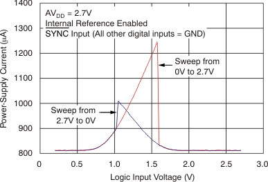 Figure 103. Power-Supply Current vs Logic Input Voltage
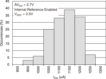 Figure 105. Power-Supply Current Histogram
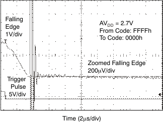 Figure 107. Full-Scale Settling Time: 2.7-V Falling Edge
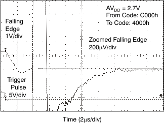 Figure 109. Half-Scale Settling Time: 2.7-V Falling Edge
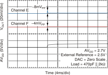 Figure 111. Power-On Glitch Reset to Zero Scale
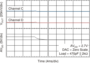 Figure 113. Power-Off Glitch
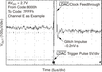 Figure 115. Glitch Energy: 2.7 V, 1-LSB Step, Falling Edge
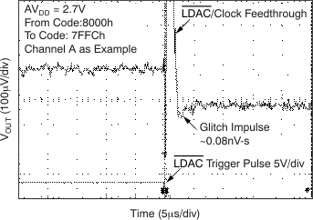 Figure 117. Glitch Energy: 2.7 V, 4-LSB Step, Falling Edge
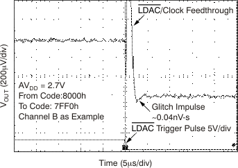 Figure 119. Glitch Energy: 2.7 V, 16-LSB Step, Falling Edge