ZHCSHR5C March   2018  – September 2019 TUSB1064

PRODUCTION DATA.  

  1. 特性
  2. 应用
  3. 说明
    1.     Device Images
      1.      简化电路原理图
      2.      TUSB1064 使用示例
  4. 修订历史记录
  5. Pin Configuration and Functions
    1.     Pin Functions
  6. Specifications
    1. 6.1 Absolute Maximum Ratings
    2. 6.2 ESD Ratings
    3. 6.3 Recommended Operating Conditions
    4. 6.4 Thermal Information
    5. 6.5 ELECTRICAL CHARACTERISTICS
    6. 6.6 Switching Characteristics
    7. 6.7 Timing Requirements
    8. 6.8 Typical Characteristics
  7. Parameter Measurement Information
  8. Detailed Description
    1. 8.1 Overview
    2. 8.2 Functional Block Diagram
    3. 8.3 Feature Description
      1. 8.3.1 USB 3.1
      2. 8.3.2 DisplayPort
      3. 8.3.3 4-level Inputs
      4. 8.3.4 Receiver Linear Equalization
    4. 8.4 Device Functional Modes
      1. 8.4.1 Device Configuration in GPIO Mode
      2. 8.4.2 Device Configuration In I2C Mode
      3. 8.4.3 DisplayPort Mode
      4. 8.4.4 Linear EQ Configuration
      5. 8.4.5 USB3.1 Modes
      6. 8.4.6 Operation Timing – Power Up
    5. 8.5 Programming
    6. 8.6 Register Maps
      1. 8.6.1 General Register (address = 0x0A) [reset = 00000001]
        1. Table 11. General Registers
      2. 8.6.2 DisplayPort Control/Status Registers (address = 0x10) [reset = 00000000]
        1. Table 12. DisplayPort Control/Status Registers (0x10)
      3. 8.6.3 DisplayPort Control/Status Registers (address = 0x11) [reset = 00000000]
        1. Table 13. DisplayPort Control/Status Registers (0x11)
      4. 8.6.4 DisplayPort Control/Status Registers (address = 0x12) [reset = 00000000]
        1. Table 14. DisplayPort Control/Status Registers (0x12)
      5. 8.6.5 DisplayPort Control/Status Registers (address = 0x13) [reset = 00000000]
        1. Table 15. DisplayPort Control/Status Registers (0x13)
      6. 8.6.6 USB3.1 Control/Status Registers (address = 0x20) [reset = 00000000]
        1. Table 16. USB3.1 Control/Status Registers (0x20)
      7. 8.6.7 USB3.1 Control/Status Registers (address = 0x21) [reset = 00000000]
        1. Table 17. USB3.1 Control/Status Registers (0x21)
      8. 8.6.8 USB3.1 Control/Status Registers (address = 0x22) [reset = 00000000]
        1. Table 18. USB3.1 Control/Status Registers (0x22)
  9. Application and Implementation
    1. 9.1 Application Information
    2. 9.2 Typical Application
      1. 9.2.1 Design Requirements
      2. 9.2.2 Detailed Design Procedure
      3. 9.2.3 Support for DisplayPort UFP_D Pin Assignment E
      4. 9.2.4 PCB Insertion Loss Curves
    3. 9.3 System Examples
      1. 9.3.1 USB 3.1 Only
      2. 9.3.2 USB 3.1 and 2 Lanes of DisplayPort
      3. 9.3.3 DisplayPort Only
  10. 10Power Supply Recommendations
  11. 11Layout
    1. 11.1 Layout Guidelines
    2. 11.2 Layout Example
  12. 12器件和文档支持
    1. 12.1 接收文档更新通知
    2. 12.2 社区资源
    3. 12.3 商标
    4. 12.4 静电放电警告
    5. 12.5 Glossary
  13. 13机械、封装和可订购信息

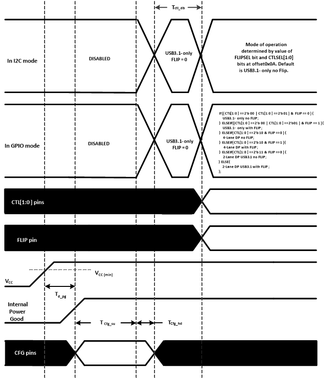
Operation Timing – Power Up

TUSB1064 TUSB564_Power_Up_Timing_SLLSSF29.gifFigure 17. Power-Up Timing

Table 8. Power-Up Timing(1)(2)

PARAMETER MIN MAX UNIT
td_pg VCC (minimum) to Internal Power Good asserted high 500 µs
tcfg_su CFG(1) pins setup(2) 50 µs
tcfg_hd CFG(1) pins hold 10 µs
tCTL_DB CTL[1:0] and FLIP pin debounce 16 ms
tVCC_RAMP VCC supply ramp requirement 0.1 100 ms
Following pins comprise CFG pins: I2C_EN, EQ[1:0], SSEQ[1:0], and DPEQ[1:0].
Recommend CFG pins are stable when VCC is at minimum value.