ZHCSHS1D May   2017  – December 2021 AWR1243

PRODUCTION DATA  

  1. 特性
  2. 应用
  3. 说明
  4. Functional Block Diagram
  5. Revision History
  6. Device Comparison
    1. 6.1 Related Products
  7. Terminal Configuration and Functions
    1. 7.1 Pin Diagram
    2. 7.2 Signal Descriptions
      1. 7.2.1 Signal Descriptions
  8. Specifications
    1. 8.1 Absolute Maximum Ratings
    2. 8.2 ESD Ratings
    3. 8.3 Power-On Hours (POH)
    4. 8.4 Recommended Operating Conditions
    5. 8.5 Power Supply Specifications
    6. 8.6 Power Consumption Summary
    7. 8.7 RF Specification
    8. 8.8 Thermal Resistance Characteristics for FCBGA Package [ABL0161]
    9. 8.9 Timing and Switching Characteristics
      1. 8.9.1 Power Supply Sequencing and Reset Timing
      2. 8.9.2 Synchronized Frame Triggering
      3. 8.9.3 Input Clocks and Oscillators
        1. 8.9.3.1 Clock Specifications
      4. 8.9.4 Multibuffered / Standard Serial Peripheral Interface (MibSPI)
        1. 8.9.4.1 Peripheral Description
          1. 8.9.4.1.1 SPI Timing Conditions
          2. 8.9.4.1.2 SPI Peripheral Mode Switching Parameters (SPICLK = input, SPISIMO = input, and SPISOMI = output)
          3. 8.9.4.1.3 SPI Peripheral Mode Timing Requirements (SPICLK = input, SPISIMO = input, and SPISOMI = output)
        2. 8.9.4.2 Typical Interface Protocol Diagram (Peripheral Mode)
      5. 8.9.5 LVDS Interface Configuration
        1. 8.9.5.1 LVDS Interface Timings
      6. 8.9.6 General-Purpose Input/Output
        1. 8.9.6.1 Switching Characteristics for Output Timing versus Load Capacitance (CL)
      7. 8.9.7 Camera Serial Interface (CSI)
        1. 8.9.7.1 CSI Switching Characteristics
  9. Detailed Description
    1. 9.1 Overview
    2. 9.2 Functional Block Diagram
    3. 9.3 Subsystems
      1. 9.3.1 RF and Analog Subsystem
        1. 9.3.1.1 Clock Subsystem
        2. 9.3.1.2 Transmit Subsystem
        3. 9.3.1.3 Receive Subsystem
      2. 9.3.2 Host Interface
    4. 9.4 Other Subsystems
      1. 9.4.1 ADC Data Format Over CSI2 Interface
  10. 10Monitoring and Diagnostics
    1. 10.1 Monitoring and Diagnostic Mechanisms
  11. 11Applications, Implementation, and Layout
    1. 11.1 Application Information
    2. 11.2 Short-, Medium-, and Long-Range Radar
    3. 11.3 Reference Schematic
  12. 12Device and Documentation Support
    1. 12.1 Device Nomenclature
    2. 12.2 Tools and Software
    3. 12.3 Documentation Support
    4. 12.4 支持资源
    5. 12.5 Trademarks
    6. 12.6 Electrostatic Discharge Caution
    7. 12.7 术语表
  13. 13Mechanical, Packaging, and Orderable Information
    1. 13.1 Packaging Information
    2. 13.2 Tray Information for

Power Supply Sequencing and Reset Timing

The AWR1243 device expects all external voltage rails and SOP lines to be stable before reset is deasserted. Figure 8-2 describes the device wake-up sequence.
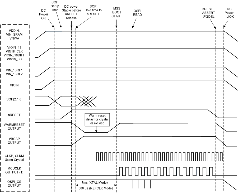
GUID-A2C4F428-E2A1-4364-8C88-4DBCECC39E8A-low.gif Figure 8-2 Device Wake-up Sequence