ZHCSHU2B March   2018  – October 2018 TPS7A10

PRODUCTION DATA.  

  1. 特性
  2. 应用
  3. 说明
    1.     Device Images
      1.      压降与 IOUT 和温度间的关系(YKA 封装)
      2.      典型应用电路
  4. 修订历史记录
  5. Pin Configuration and Functions
    1.     Pin Functions
  6. Specifications
    1. 6.1 Absolute Maximum Ratings
    2. 6.2 ESD Ratings
    3. 6.3 Recommended Operating Conditions
    4. 6.4 Thermal Information
    5. 6.5 Electrical Characteristics
    6. 6.6 Typical Characteristics
  7. Detailed Description
    1. 7.1 Overview
    2. 7.2 Functional Block Diagram
    3. 7.3 Feature Description
      1. 7.3.1 Excellent Transient Response
      2. 7.3.2 Global Undervoltage Lockout (UVLO)
      3. 7.3.3 Active Discharge
      4. 7.3.4 Enable
      5. 7.3.5 Sequencing Requirement
      6. 7.3.6 Internal Foldback Current Limit
      7. 7.3.7 Thermal Shutdown
    4. 7.4 Device Functional Modes
      1. 7.4.1 Normal Mode
      2. 7.4.2 Dropout Mode
      3. 7.4.3 Disable Mode
  8. Application and Implementation
    1. 8.1 Application Information
      1. 8.1.1 Recommended Capacitor Types
      2. 8.1.2 Input and Output Capacitor Requirements
      3. 8.1.3 Load Transient Response
      4. 8.1.4 Dropout Voltage
      5. 8.1.5 Behavior During Transition From Dropout Into Regulation
      6. 8.1.6 Undervoltage Lockout Circuit Operation
      7. 8.1.7 Power Dissipation (PD)
        1. 8.1.7.1 Estimating Junction Temperature
        2. 8.1.7.2 Recommended Area for Continuous Operation
    2. 8.2 Typical Application
      1. 8.2.1 Design Requirements
      2. 8.2.2 Detailed Design Procedure
        1. 8.2.2.1 Input Current
        2. 8.2.2.2 Thermal Dissipation
      3. 8.2.3 Application Curve
  9. Power Supply Recommendations
  10. 10Layout
    1. 10.1 Layout Guidelines
    2. 10.2 Layout Examples
  11. 11器件和文档支持
    1. 11.1 器件支持
      1. 11.1.1 开发支持
        1. 11.1.1.1 评估模块
        2. 11.1.1.2 Spice 模型
      2. 11.1.2 器件命名规则
    2. 11.2 文档支持
      1. 11.2.1 相关文档
    3. 11.3 接收文档更新通知
    4. 11.4 社区资源
    5. 11.5 商标
    6. 11.6 静电放电警告
    7. 11.7 术语表
  12. 12机械、封装和可订购信息

Recommended Area for Continuous Operation

The operational area of an LDO is limited by the dropout voltage, output current, junction temperature, and input voltage. The recommended area for continuous operation for a linear regulator is shown in Figure 41, and can be separated into the following regions:

  • Dropout voltage limits the minimum differential voltage between the input and the output (VIN – VOUT) at a given output current level.
  • The rated output currents limits the maximum recommended output current level. Exceeding this rating causes the device to fall out of specification.
  • The rated junction temperature limits the maximum junction temperature of the device. Exceeding this rating causes the device to fall out of specification and reduces long-term reliability.
    • Equation 5 provides the shape of the slope. The slope is nonlinear because the maximum rated junction temperature of the LDO is controlled by the power dissipation across the LDO, thus when VIN – VOUT increases, the output current must decrease.
  • The rated input voltage range governs both the minimum and maximum of VIN – VOUT.
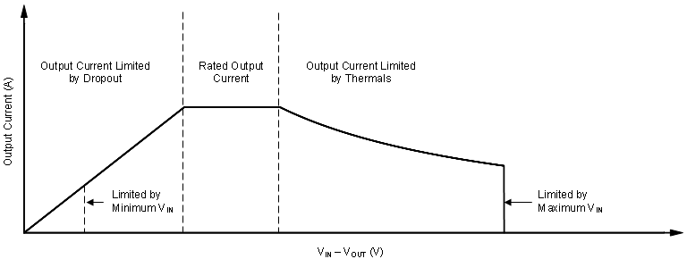
TPS7A10 ai_SOA_Curve_Explanation_SBVS267.gifFigure 41. Region Description of Continuous Operation Regime