ZHCSHV3A March 2018 – November 2018 LMX8410L
PRODUCTION DATA.
- 1 特性
- 2 应用
- 3 说明
- 4 修订历史记录
- 5 Pin Configuration and Functions
- 6 Specifications
-
7 Detailed Description
- 7.1 Overview
- 7.2 Functional Block Diagram
- 7.3
Feature Description
- 7.3.1 Device Configurations and Feature Description
- 7.4 Device Functional Modes
- 7.5 Programming
- 7.6
Register Map
- 7.6.1 R0 Register (Address = 0x0) [reset = X]
- 7.6.2 R1 Register (Address = 0x1) [reset = 0x3]
- 7.6.3 R2 Register (Address = 0x2) [reset = X]
- 7.6.4 R9 Register (Address = 0x9) [reset = X]
- 7.6.5 R10 Register (Address = 0xA) [reset = 0x80]
- 7.6.6 R11 Register (Address = 0xB) [reset = 0x10]
- 7.6.7 R14 Register (Address = 0xE) [reset = 0x70]
- 7.6.8 R36 Register (Address = 0x24) [reset = 0x64]
- 7.6.9 R37 Register (Address = 0x25) [reset = 0x200]
- 7.6.10 R38 Register (Address = 0x26) [reset = 0x0]
- 7.6.11 R39 Register (Address = 0x27) [reset = 0x2710]
- 7.6.12 R40 Register (Address = 0x28) [reset = 0x0]
- 7.6.13 R41 Register (Address = 0x29) [reset = 0x0]
- 7.6.14 R42 Register (Address = 0x2A) [reset = 0x0]
- 7.6.15 R43 Register (Address = 0x2B) [reset = 0x0]
- 7.6.16 R44 Register (Address = 0x2C) [reset = 0xA2]
- 7.6.17 R46 Register (Address = 0x2E) [reset = 0x1]
- 7.6.18 R58 Register (Address = 0x3A) [reset = 0x8000]
- 7.6.19 R59 Register (Address = 0x3B) [reset = 0x1]
- 7.6.20 R69 Register (Address = 0x45) [reset = 0x0]
- 7.6.21 R70 Register (Address = 0x46) [reset = 0xC350]
- 7.6.22 R75 Register (Address = 0x4B) [reset = 0x0]
- 7.6.23 R78 Register (Address = 0x4E) [reset = 0x0]
- 7.6.24 R79 Register (Address = 0x4F) [reset = 0x7000]
- 7.6.25 R80 Register (Address = 0x50) [reset = 0xA]
- 7.6.26 R81 Register (Address = 0x51) [reset = 0x0]
- 7.6.27 R82 Register (Address = 0x52) [reset = 0x23]
- 7.6.28 R83 Register (Address = 0x53) [reset = 0x2000]
- 7.6.29 R84 Register (Address = 0x54) [reset = 0x1900]
- 7.6.30 R88 Register (Address = 0x58) [reset = 0x0]
- 7.6.31 R94 Register (Address = 0x5E) [reset = 0x8080]
- 7.6.32 R95 Register (Address = 0x5F) [reset = X]
- 7.6.33 R103 Register (Address = 0x67) [reset = X]
- 7.6.34 R110 Register (Address = 0x6E) [reset = X]
- 7.6.35 R111 Register (Address = 0x6F) [reset = 0x0]
- 7.6.36 R112 Register (Address = 0x70) [reset = 0x0]
- 7.6.37 R121 Register (Address = 0x79) [reset = 0x0]
- 7.6.38 R123 Register (Address = 0x7B) [reset = 0x3]
- 7.6.39 R126 Register (Address = 0x7E) [reset = X]
- 8 Application and Implementation
- 9 Power Supply Recommendations
- 10Layout
- 11器件和文档支持
- 12机械、封装和可订购信息
6.6 Timing Requirements
| MIN | NOM | MAX | UNIT | ||
|---|---|---|---|---|---|
| SYNC | |||||
| tSETUP | Setup time for pin relative to OSCIN rising edge | 2.5 | ns | ||
| tHOLD | Hold time for pin relative to OSCIN rising edge | 2 | ns | ||
| DIGITAL WRITE INTERFACE(1) | |||||
| FSPI_WRITE | SPI write speed | 50 | MHz | ||
| tES | Clock to enable low time | 5 | ns | ||
| tCS | Data to clock setup time | 2 | ns | ||
| tCH | Data to clock hold time | 2 | ns | ||
| tCWH | Clock pulse width high | 5 | ns | ||
| tCWL | Clock pulse width low | 10 | ns | ||
| tCES | Enable to clock setup time | 10 | ns | ||
| tEWH | Enable pulse width high | 10 | ns | ||
| DIGITAL READBACK INTERFACE(2) | |||||
| FSPI_READ | SPI readback speed | 50 | MHz | ||
| tES | Clock to enable low time | 10 | ns | ||
| tCS | Clock to data wait time | 10 | ns | ||
| tCWH | Clock pulse width high | 10 | ns | ||
| tCWL | Clock pulse width low | 10 | ns | ||
| tCES | Enable to clock setup time | 10 | ns | ||
| tEWH | Enable pulse width high | 10 | ns | ||
 Figure 1. Serial Data Input Timing Diagram
 There are several other considerations for writing on the SPI:
- The R/W bit must be set to 0.
- The signal on the SDI pin is clocked into a shift register on each rising edge of the SCK pin.
- The CSB must be held low for data to be clocked. Device ignores clock pulses if CSB is held high.
- The CSB transition from high to low must occur when SCK is low.
- When SCK and SDI lines are shared between devices, TI recommends holding the CSB line high on any devices besides the intended programming target.
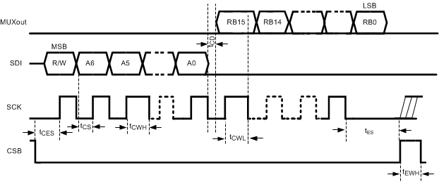
 Figure 2. Serial Data Readback Timing Diagram
 There are several other considerations for SPI readback:
- The R/W bit must be set to 1.
- The MUXOUT pin is always for the address portion of the transaction.
- The address on the SDI pin is clocked into a shift register on each rising edge of the SCK pin.
- The data portion of the transaction on the SDI line is always ignored.
- The data on the MUXOUT pin should be considered valid on each rising edge of the SCK pin, provided all timing requirements are met.
- All CSB considerations for SPI writing also apply to SPI readback.