ZHCSHV9A March   2018  – January 2024 LMR14010A

PRODUCTION DATA  

  1.   1
  2. 特性
  3. 应用
  4. 说明
  5. Pin Configuration and Functions
  6. Specifications
    1. 5.1 Absolute Maximum Ratings
    2. 5.2 ESD Ratings
    3. 5.3 Recommended Operating Conditions
    4. 5.4 Thermal Information
    5. 5.5 Electrical Characteristics
    6. 5.6 Typical Characteristics
  7. Detailed Description
    1. 6.1 Overview
    2. 6.2 Functional Block Diagram
    3. 6.3 Feature Description
      1. 6.3.1 Fixed Frequency PWM Control
      2. 6.3.2 Bootstrap Voltage (CB)
      3. 6.3.3 Setting the Output Voltage
      4. 6.3.4 Enable ( SHDN ) and VIN Undervoltage Lockout
      5. 6.3.5 Current Limit
      6. 6.3.6 Thermal Shutdown
    4. 6.4 Device Functional Modes
      1. 6.4.1 Continuous Conduction Mode
      2. 6.4.2 Eco-mode
  8. Application and Implementation
    1. 7.1 Application Information
    2. 7.2 Typical Application
      1. 7.2.1 Design Requirements
        1. 7.2.1.1 Step-By-Step Design Procedure
      2. 7.2.2 Detailed Design Procedure
        1. 7.2.2.1 Custom Design With WEBENCH® Tools
        2. 7.2.2.2 Output Inductor Selection
        3. 7.2.2.3 Output Capacitor Selection
        4. 7.2.2.4 Schottky Diode Selection
        5. 7.2.2.5 Input Capacitor Selection
        6. 7.2.2.6 Bootstrap Capacitor Selection
      3. 7.2.3 Application Performance Curves
    3. 7.3 Power Supply Recommendations
    4. 7.4 Layout
      1. 7.4.1 Layout Guidelines
      2. 7.4.2 Layout Example
  9. Device and Documentation Support
    1. 8.1 Device Support
      1. 8.1.1 Development Support
        1. 8.1.1.1 Custom Design With WEBENCH® Tools
    2. 8.2 接收文档更新通知
    3. 8.3 支持资源
    4. 8.4 Trademarks
    5. 8.5 静电放电警告
    6. 8.6 术语表
  10. Revision History
  11. 10Mechanical, Packaging, and Orderable Information

Application Performance Curves

Unless otherwise noted, VIN = 12 V, L = 22 µH, COUT = 22 µF, TA = 25°C.
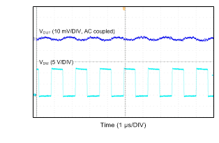
LMR14010A Switching Node and Output Voltage Waveform (VIN = 12 V, VOUT = 5 V, ILoad = 1 A)Figure 7-2 Switching Node and Output Voltage Waveform (VIN = 12 V, VOUT = 5 V, ILoad = 1 A)
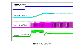
LMR14010A Start-up Waveform (VIN = 18 V, VOUT= 12 V, ILoad= 800 mA)Figure 7-4 Start-up Waveform (VIN = 18 V, VOUT= 12 V, ILoad= 800 mA)
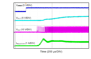
LMR14010A Start-Up Waveform (VIN = 12 V, VOUT = 5 V, ILoad = 800 mA)Figure 7-6 Start-Up Waveform (VIN = 12 V, VOUT = 5 V, ILoad = 800 mA)
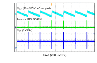
LMR14010A Eco-mode Operation
                            (VIN = 12 V, VOUT = 5 V, No Load)Figure 7-8 Eco-mode Operation (VIN = 12 V, VOUT = 5 V, No Load)
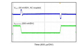
LMR14010A Load Transient Between 0.1 A and 1 A (VIN= 12 V, VOUT = 5 V)Figure 7-3 Load Transient Between 0.1 A and 1 A (VIN= 12 V, VOUT = 5 V)
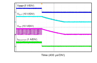
LMR14010A Shutdown Waveform (VIN = 18 V, VOUT = 12 V, ILoad= 800 mA)Figure 7-5 Shutdown Waveform (VIN = 18 V, VOUT = 12 V, ILoad= 800 mA)
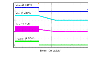
LMR14010A Shutdown Waveform (VIN = 12 V, VOUT = 5 V, ILoad= 800 mA)Figure 7-7 Shutdown Waveform (VIN = 12 V, VOUT = 5 V, ILoad= 800 mA)