ZHCSHW1C March 2018 – January 2019 ADS1260 , ADS1261
PRODUCTION DATA.
- 1 特性
- 2 应用
- 3 说明
- 4 修订历史记录
- 5 Device Comparison Table
- 6 Pin Configuration and Functions
- 7 Specifications
- 8 Parameter Measurement Information
-
9 Detailed Description
- 9.1 Overview
- 9.2 Functional Block Diagram
- 9.3 Feature Description
- 9.4
Device Functional Modes
- 9.4.1 Conversion Control
- 9.4.2 Chop Mode
- 9.4.3 AC-Excitation Mode
- 9.4.4 ADC Clock Mode
- 9.4.5 Power-Down Mode
- 9.4.6 Reset
- 9.4.7 Calibration
- 9.5 Programming
- 9.6
Register Map
- 9.6.1 Device Identification (ID) Register (address = 00h) [reset = xxh]
- 9.6.2 Device Status (STATUS) Register (address = 01h) [reset = 01h]
- 9.6.3 Mode 0 (MODE0) Register (address = 02h) [reset = 24h]
- 9.6.4 Mode 1 (MODE1) Register (address = 03h) [reset = 01h]
- 9.6.5 Mode 2 (MODE2) Register (address = 04h) [reset = 00h]
- 9.6.6 Mode 3 (MODE3) Register (address = 05h) [reset = 00h]
- 9.6.7 Reference Configuration (REF) Register (address = 06h) [reset = 05h]
- 9.6.8 Offset Calibration (OFCALx) Registers (address = 07h, 08h, 09h) [reset = 00h, 00h, 00h]
- 9.6.9 Full-Scale Calibration (FSCALx) Registers (address = 0Ah, 0Bh, 0Ch) [reset = 00h, 00h, 40h]
- 9.6.10 IDAC Multiplexer (IMUX) Register (address = 0Dh) [reset = FFh]
- 9.6.11 IDAC Magnitude (IMAG) Register (address = 0Eh) [reset = 00h]
- 9.6.12 Reserved (RESERVED) Register (address = 0Fh) [reset = 00h]
- 9.6.13 PGA Configuration (PGA) Register (address = 10h) [reset = 00h]
- 9.6.14 Input Multiplexer (INPMUX) Register (address = 11h) [reset = FFh]
- 9.6.15 Input Bias (INPBIAS) Register (address = 12h) [reset = 00h]
- 10Application and Implementation
- 11Power Supply Recommendations
- 12Layout
- 13器件和文档支持
- 14机械、封装和可订购信息
9.3.7 General-Purpose Input/Outputs (GPIOs)
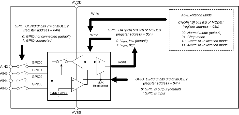
The ADS1261 and ADS1261B devices provide four GPIO pins, GPIO0 through GPIO3. The GPIOs are digital inputs/outputs that are referenced to analog AVDD and AVSS. The GPIOs are read and written by the GPIO_DAT bits of register MODE3. The GPIOs are multiplexed with analog inputs AIN2 to AIN5. As shown in Figure 59, the GPIOs have a series of programming registers. Bits GPIO_CON[3:0] connect the GPIOs to the associated pin (1 = connect). Bits GPIO_DIR program the direction of the GPIOs; (0 = output, 1 = input). The input voltage threshold is the voltage value between AVDD and AVSS. Bits GPIO_DAT[3:0] are the data values for the GPIOs. Observe that if a GPIO pin is programmed as an output, the value read is the value previously written to the register data, not the actual state of the pin.
The GPIOs also provide the AC-excitation drive signals. AC-excitation mode override the GPIO register data values. See the AC-Excitation Mode section for details.
 Figure 59. GPIO Block Diagram