ZHCSHX8D September 2017 – October 2019 TPS50601A-SP
PRODUCTION DATA.
- 1 特性
- 2 应用
- 3 说明
- 4 修订历史记录
- 5 Pin Configuration and Functions
- 6 Specifications
-
7 Detailed Description
- 7.1 Overview
- 7.2 Functional Block Diagram
- 7.3
Feature Description
- 7.3.1 VIN and Power VIN Pins (VIN and PVIN)
- 7.3.2 Voltage Reference
- 7.3.3 Adjusting the Output Voltage
- 7.3.4 Safe Start-Up Into Prebiased Outputs
- 7.3.5 Error Amplifier
- 7.3.6 Slope Compensation
- 7.3.7 Enable and Adjust UVLO
- 7.3.8 Adjustable Switching Frequency and Synchronization (SYNC)
- 7.3.9 Slow Start (SS/TR)
- 7.3.10 Power Good (PWRGD)
- 7.3.11 Sequencing (SS/TR)
- 7.3.12 Output Overvoltage Protection (OVP)
- 7.3.13 Overcurrent Protection
- 7.3.14 Thermal Shutdown
- 7.3.15 Turn-On Behavior
- 7.3.16 Small Signal Model for Frequency Compensation
- 7.4 Device Functional Modes
- 8 Application and Implementation
- 9 Power Supply Recommendations
- 10Layout
- 11器件和文档支持
- 12机械、封装和可订购信息
7.3.8 Adjustable Switching Frequency and Synchronization (SYNC)
The switching frequency of the device supports three modes of operations. The modes of operation are set by the conditions on the RT and SYNC pins. At a high level, these modes can be described as master, internal oscillator, and external synchronization modes.
In master mode, the RT pin should be left floating; the internal oscillator is set to 500 kHz, and the SYNC pin is set as an output clock. The SYNC output is in phase with respect to the internal oscillator. SYNC out signal level is the same as VIN level with 50% duty cycle. SYNC signal feeding the slave module, which is in phase with the master clock, gets internally inverted (180° out of phase with the master clock) internally in the slave module.
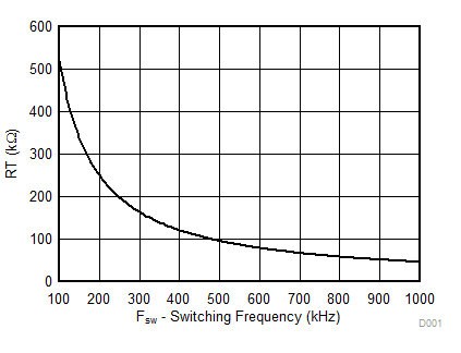
In internal oscillator mode, a resistor is connected between the RT pin and GND. The SYNC pin requires a 10-kΩ resistor to GND for this mode to be effective. The switching frequency of the device is adjustable from 100 kHz to 1 MHz by placing a maximum of 510 kΩ and a minimum of 47 kΩ respectively. To determine the RT resistance for a given switching frequency, use Equation 4 or the curve in Figure 18. To reduce the solution size, the designer should set switching frequency as high as possible, but consider the tradeoffs of supply efficiency and minimum controllable on-time.

where
- RT in kΩ
- fSW in kHz
 Figure 18. RT vs Switching Frequency
 When operating the converter in internal oscillator mode (internal oscillator determines the switching frequency (500 kHz) default), the synchronous pin becomes the output and there is a phase inversion. When trying to parallel with another converter, the RT pin of the second (slave) converter must have its RT pin populated such that the converter frequency of the slave converter must be within ±5% of the master converter. This is required because the RT pin also sets the proper operation of slope compensation.
In external synchronization mode, a resistor is connected between the RT pin and GND. The SYNC pin requires a toggling signal for this mode to be effective. The switching frequency of the device goes 1:1 with that of SYNC pin. External system clock-user supplied sync clock signal determines the switching frequency. If no external clock signal is detected for 20 µs, then TPS50601A-SP transitions to its internal clock, which is typically 500 kHz. An external synchronization using an inverter to obtain phase inversion is necessary. RT values of the master and slave converter must be within ±5% of the external synchronization frequency. This is necessary for proper slope compensation. A resistance in the RT pin is required for proper operation of the slope compensation circuit. To determine the RT resistance for a given switching frequency, use Equation 4 or the curve in Figure 18.
These modes are described in Table 3.