ZHCSHY7A April 2018 – May 2018 UCC28742
PRODUCTION DATA.
- 1 特性
- 2 应用
- 3 说明
- 4 修订历史记录
- 5 Pin Configuration and Functions
- 6 Specifications
-
7 Detailed Description
- 7.1 Overview
- 7.2 Functional Block Diagram
- 7.3 Feature Description
- 7.4 Device Functional Modes
-
8 Applications and Implementation
- 8.1 Application Information
- 8.2
Typical Application
- 8.2.1 Design Requirements
- 8.2.2
Detailed Design Procedure
- 8.2.2.1 Custom Design With WEBENCH® Tools
- 8.2.2.2 VDD Capacitance, CDD
- 8.2.2.3 VDD Start-Up Resistance, RSTR
- 8.2.2.4 Input Bulk Capacitance and Minimum Bulk Voltage
- 8.2.2.5 Transformer Turns Ratio, Inductance, Primary-Peak Current
- 8.2.2.6 Transformer Parameter Verification
- 8.2.2.7 VS Resistor Divider and Line Compensation
- 8.2.2.8 Standby Power Estimate
- 8.2.2.9 Output Capacitance
- 8.2.2.10 Feedback Loop Design Consideration
- 8.2.3 Application Curves
- 8.3 Do's and Don'ts
- 9 Power Supply Recommendations
- 10Layout
- 11器件和文档支持
- 12机械、封装和可订购信息
7.3.4 Constant Current Limit and Delayed Shutdown
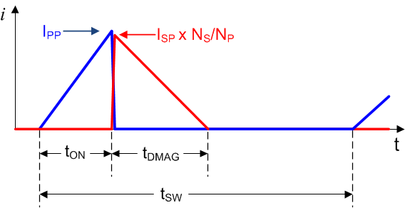
Timing information at the VS pin and current information at the CS pin allow accurate regulation of the secondary constant current limit, CCL, thus to achieve load over-current protection. The control law dictates that as power is increased in CV regulation and approaching CCL the primary-peak current is at IPP(max). Referring to Figure 13 below, the primary peak current (IPP), turns-ratio (NS/NP), secondary demagnetization time (tDMAG), and switching period (tSW) determine the secondary average output current. Ignoring leakage inductance effects, the average output current is given by Equation 5. By regulating the secondary rectifier conduction duty cycle, the output current limit is achieved for given IPP and transformer turns-ratio. When the load increases, the secondary-side rectifier conduction duty cycle keep increasing. Once this duty cycle reaches preset value of 0.475, the converter switching frequency stops increasing and starts adjusting to reduce and maintain 0.475 secondary-side duty cycle. Therefore, the output constant current limit is achieved. Because the current is kept constant, the increasing load results in lower output voltage.

 Figure 13. Transformer Currents
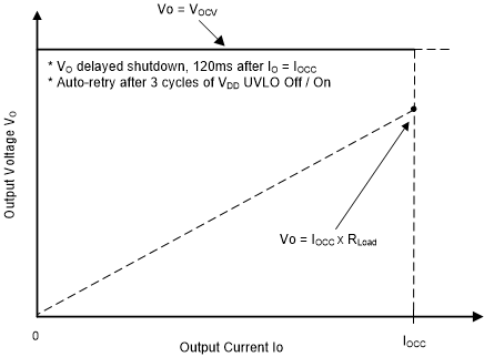
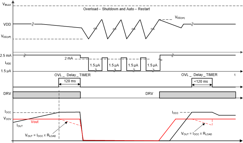
 As shown in Figure 14 below, CV mode operation is from IO = 0 to < IOCC; at IO = IOCC, the operation enters constant current limit mode and VO starts to drop as the load resistance becomes further lower while IO is maintained at IOCC for a time interval specified by tOVL_TIME typically 120 ms then DRV stops to achieve converter output delayed shutdown. During the 120-ms timing interval, if load IO reduces to < IOCC, the timer will be reset and no shutdown will occur. The V-I curve corresponding to the operation is shown in Figure 14, and the delayed shutdown timing diagram is shown in Figure 15. Note (1) The timer tOVL_TIME is triggered whenever IO reaches IOCC and reset when IO drops to < IOCC before 120ms-time-out. (2) during 120-ms time interval, when load resistance becomes so low during constant current interval that causes the device VDD to reach its VVDD(off) and then the shutdown will be through VDD undervoltage lockout instead of through Constant Current Limit and Delayed Shutdown. In such a case, the shutdown can happen before 120ms timer out.
 Figure 14. Typical Target Output V-I Characteristics
  Figure 15. Output Delayed Shutdown Timing