ZHCSHY7A April 2018 – May 2018 UCC28742
PRODUCTION DATA.
- 1 特性
- 2 应用
- 3 说明
- 4 修订历史记录
- 5 Pin Configuration and Functions
- 6 Specifications
-
7 Detailed Description
- 7.1 Overview
- 7.2 Functional Block Diagram
- 7.3 Feature Description
- 7.4 Device Functional Modes
-
8 Applications and Implementation
- 8.1 Application Information
- 8.2
Typical Application
- 8.2.1 Design Requirements
- 8.2.2
Detailed Design Procedure
- 8.2.2.1 Custom Design With WEBENCH® Tools
- 8.2.2.2 VDD Capacitance, CDD
- 8.2.2.3 VDD Start-Up Resistance, RSTR
- 8.2.2.4 Input Bulk Capacitance and Minimum Bulk Voltage
- 8.2.2.5 Transformer Turns Ratio, Inductance, Primary-Peak Current
- 8.2.2.6 Transformer Parameter Verification
- 8.2.2.7 VS Resistor Divider and Line Compensation
- 8.2.2.8 Standby Power Estimate
- 8.2.2.9 Output Capacitance
- 8.2.2.10 Feedback Loop Design Consideration
- 8.2.3 Application Curves
- 8.3 Do's and Don'ts
- 9 Power Supply Recommendations
- 10Layout
- 11器件和文档支持
- 12机械、封装和可订购信息
7.3.6 Start-Up Operation
Upon application of input voltage to the converter, the start up resistance connected to VDD from the bulk capacitor voltage (VBULK) charges the VDD capacitor. During charging of the VDD capacitor, the device supply current is typical 1.5 µA. When VDD reaches the 21.6-V UVLO turn-on threshold, the controller is enabled and the converter starts switching. The peak-primary currents with initial three cycles are limited to IPP(min). This allows sensing any initial input or output faults with minimal power delivery. When confirmed that the input voltage is above the programmed converter turn-on voltage and with no faults detected, the start-up process proceeds and normal power conversion follows. The converter remains in discontinuous conduction mode operation during charging of the output capacitor(s), maintaining a constant output current until the output voltage is in regulation.
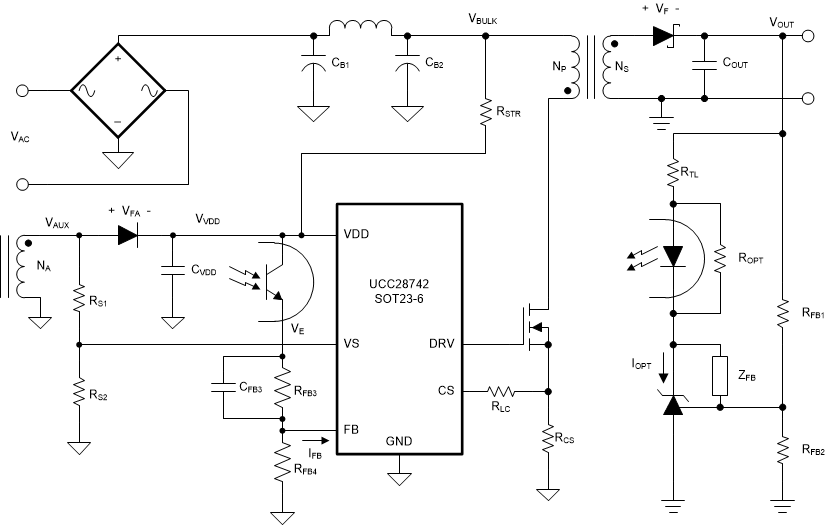
A commonly used initial power-on approach for UCC28742 is to use a start-up resistor, RSTR, to tie VDD to VBULK, as show in Figure 17. With this approach, the VDD pin is connected to a bypass capacitor to ground and a start-up resistance to the input bulk capacitor (+) terminal. The VDD turn-on UVLO threshold is 21.6 V (VVDD(on)) and turn-off UVLO threshold is 7.8 V (VVDD(off)), with an available operating range up to 35 V. The additional VDD headroom up to 35 V allows for VDD to rise due to the leakage energy delivered to the VDD capacitor in heavy-load conditions. Also, the wide VDD range provides the advantage of selecting a relatively small VDD capacitor and high-value startup resistance to minimize no-load standby power loss in the startup resistor.
The RSTR value has an effect to power-on delay time and no-load standby power losses. Both are usually part of the design specifications. Increasing RSTR reduces standby power losses while also increasing power-on delay time. A typical range of RSTR is between 1 MΩ and 10 MΩ as a good initial design point for off-line AC-to-DC adapters. Due to the limited voltage rating, RSTR is normally implemented by two or three resistors in series.
 Figure 17. Power-On with Start-Up Resistor