ZHCSHZ8B april 2018 – february 2023 TPS62147 , TPS62148
PRODUCTION DATA
- 1 特性
- 2 应用
- 3 说明
- 4 Revision History
- 5 Device Comparison Table
- 6 Pin Configuration and Functions
- 7 Specifications
- 8 Parameter Measurement Information
-
9 Detailed Description
- 9.1 Overview
- 9.2 Functional Block Diagram
- 9.3 Feature Description
- 9.4
Device Functional Modes
- 9.4.1 Pulse Width Modulation (PWM) Operation
- 9.4.2 Power Save Mode Operation (PWM/PFM)
- 9.4.3 100% Duty-Cycle Operation
- 9.4.4 Current Limit And Short Circuit Protection (for TPS62148)
- 9.4.5 HICCUP Current Limit And Short Circuit Protection (for TPS62147)
- 9.4.6 Soft Start / Tracking (SS/TR)
- 9.4.7 Output Discharge Function (TPS62148 only)
- 9.4.8 Starting into a Pre-Biased Load
- 10Application and Implementation
- 11Device and Documentation Support
- 12Mechanical, Packaging, and Orderable Information
8.1 Schematic
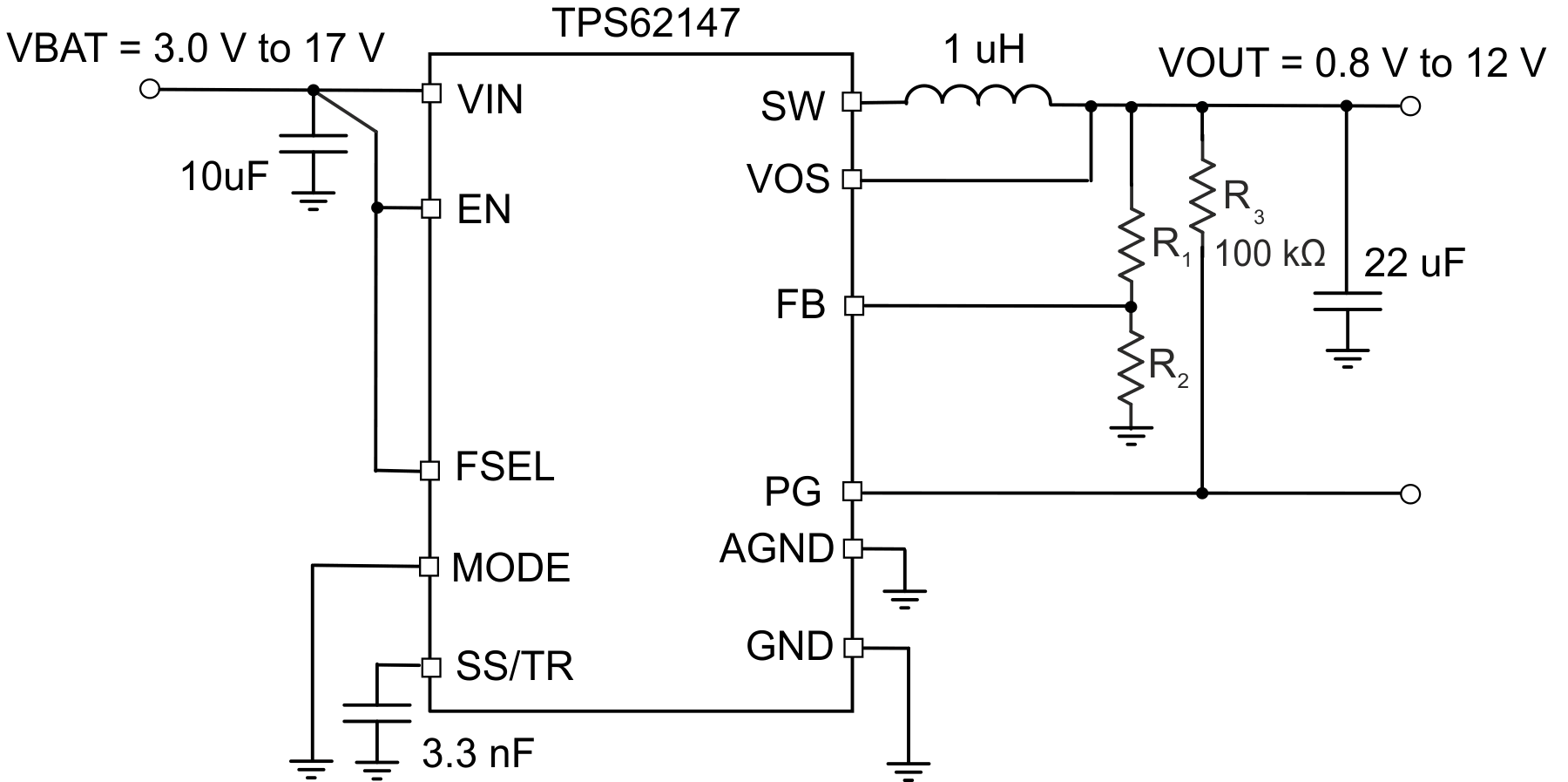
 Figure 8-1 Measurement Setup with FSEL = high
Table 8-1 List of Components for FSEL = high (fsw = 2.5 MHz)
| REFERENCE | DESCRIPTION | MANUFACTURER |
|---|---|---|
| IC | 17 V, 2 A Step-Down Converter | TPS62147; Texas Instruments |
| L | 1 µH inductor | XFL4020-102; Coilcraft |
| CIN | 10 µF, 25 V, Ceramic, 0805 | TMK212BBJ106MG-T; Taiyo Yuden |
| COUT | 2 × 10 µF, 16 V, Ceramic, 0805; all VOUT except 9 V and 1.2 V | EMK212BBJ106MG-T; Taiyo Yuden |
| COUT | 3 × 10 µF, 16 V, Ceramic, 0805 for VOUT = 1.2 V | EMK212BBJ106MG-T; Taiyo Yuden |
| COUT | 4 × 10 µF, 16 V, Ceramic, 0805 for VOUT = 9 V | EMK212BBJ106MG-T; Taiyo Yuden |
| CSS | 3.3 nF, 10 V, Ceramic, X7R | - |
| R1 | Depending on Vout; see Table 10-4 | Standard 1% metal film |
| R2 | Depending on Vout; see Table 10-4 | Standard 1% metal film |
| R3 | 470 kΩ, Chip, 0603, 1/16 W, 1% | Standard 1% metal film |
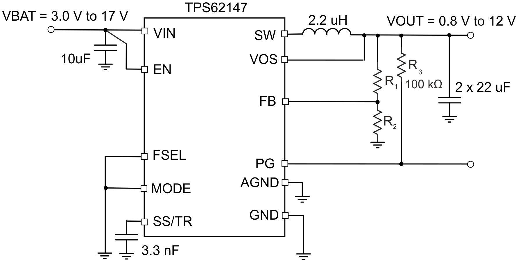
 Figure 8-2 Measurement Setup with FSEL = low
Table 8-2 List of Components for FSEL = low (fsw = 1.25 MHz)
| REFERENCE | DESCRIPTION | MANUFACTURER(1) |
|---|---|---|
| IC | 17 V, 2 A Step-Down Converter | TPS62147; Texas Instruments |
| L | 2.2 µH inductor | XFL4020-222; Coilcraft |
| CIN | 10 µF, 25 V, Ceramic, 0805 | TMK212BBJ226MG-T; Taiyo Yuden |
| COUT | 2 × 22 µF, 16 V, Ceramic, 0805; all VOUT except 9 V and 1.2 V | EMK212BBJ226MG-T; Taiyo Yuden |
| COUT | 3 × 22 µF, 16 V, Ceramic, 0805 for VOUT = 1.2 V and VOUT = 9 V | EMK212BBJ226MG-T; Taiyo Yuden |
| CSS | 3.3 nF, 10 V, Ceramic, X7R | - |
| R1 | Depending on Vout; see Table 10-4 | Standard 1% metal film |
| R2 | Depending on Vout; see Table 10-4 | Standard 1% metal film |
| R3 | 470 kΩ, Chip, 0603, 1/16 W, 1% | Standard 1% metal film |
(1) See Third-party Products Disclaimer