ZHCSI00D April 2018 – September 2020 LMR36015
PRODUCTION DATA
- 1 特性
- 2 应用
- 3 说明
- 4 Revision History
- 5 说明(续)
- 6 Device Comparison Table
- 7 Pin Configuration and Functions
- 8 Specifications
- 9 Detailed Description
-
10Application and Implementation
- 10.1 Application Information
- 10.2
Typical Application
- 10.2.1
Design 1: Low Power 24-V, 1.5-A PFM Converter
- 10.2.1.1 Design Requirements
- 10.2.1.2
Detailed Design Procedure
- 10.2.1.2.1 Custom Design With WEBENCH Tools
- 10.2.1.2.2 Choosing the Switching Frequency
- 10.2.1.2.3 Setting the Output Voltage
- 10.2.1.2.4 Inductor Selection
- 10.2.1.2.5 Output Capacitor Selection
- 10.2.1.2.6 Input Capacitor Selection
- 10.2.1.2.7 CBOOT
- 10.2.1.2.8 VCC
- 10.2.1.2.9 CFF Selection
- 10.2.1.2.10 Maximum Ambient Temperature
- 10.2.2 Application Curves
- 10.2.3 Design 2: High Density 24-V, 1.5-A FPWM Converter
- 10.2.1
Design 1: Low Power 24-V, 1.5-A PFM Converter
- 10.3 What to Do and What Not to Do
- 11Power Supply Recommendations
- 12Layout
- 13Device and Documentation Support
- 14Mechanical, Packaging, and Orderable Information
9.4.1 Auto Mode
In auto mode, the device moves between PWM and PFM as the load changes. At light loads, the regulator operates in PFM. At higher loads, the mode changes to PWM.
In PWM, the regulator operates as a constant frequency, current mode, full synchronous converter using PWM to regulate the output voltage. While operating in this mode, the output voltage is regulated by switching at a constant frequency and modulating the duty cycle to control the power to the load. This provides excellent line and load regulation and low output voltage ripple.
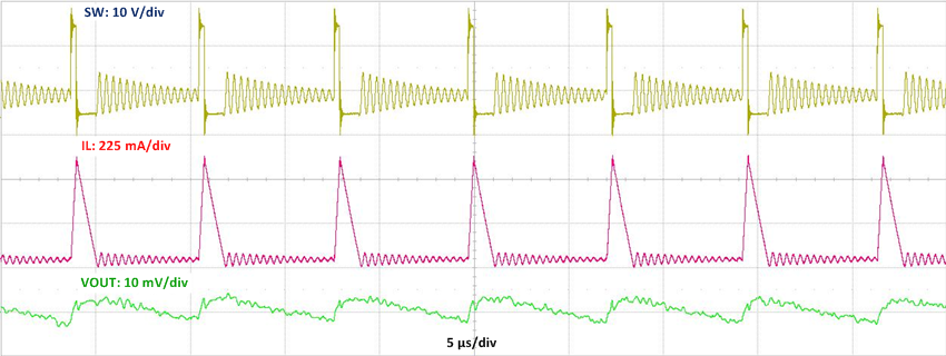
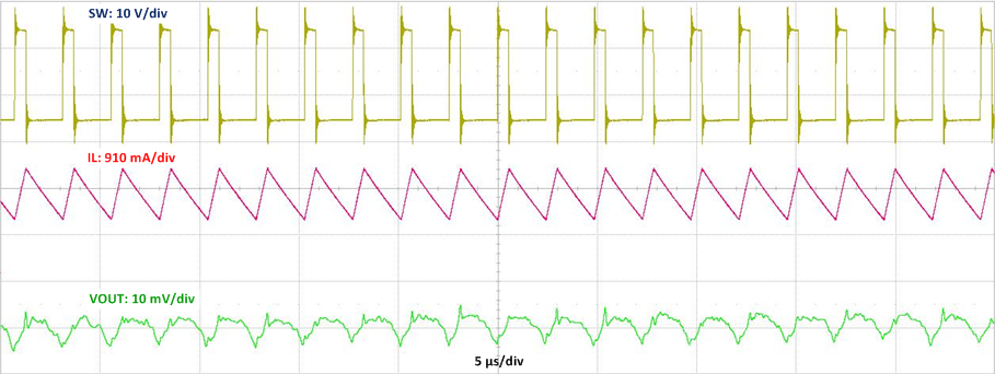
In PFM, the high-side MOSFET is turned on in a burst of one or more pulses to provide energy to the load. The duration of the burst depends on how long it takes the inductor current to reach IPEAK-MIN. The frequency of these bursts is adjusted to regulate the output, while diode emulation (DEM) is used to maximize efficiency (see Section 13.7). This mode provides high light-load efficiency by reducing the amount of input supply current required to regulate the output voltage at small loads. This trades off very good light-load efficiency for larger output voltage ripple and variable switching frequency. Also, a small increase in output voltage occurs at light loads. The actual switching frequency and output voltage ripple depend on the input voltage, output voltage, and load. Typical switching waveforms in PFM and PWM are shown in Figure 9-7 and Figure 9-8.See Section 10.2.2 for output voltage variation with load in auto mode.
 Figure 9-7 Typical PFM Switching Waveforms VIN = 24 V, VOUT = 5
V, IOUT = 200 mA
 Figure 9-8 Typical PWM Switching Waveforms VIN = 24 V, VOUT = 5
V, IOUT = 1.5 A, ƒS = 400 kHz