ZHCSI04E September 2009 – April 2018 TPS54418
PRODUCTION DATA.
- 1 特性
- 2 应用
- 3 说明
- 4 修订历史记录
- 5 Pin Configuration and Functions
- 6 Specifications
-
7 Detailed Description
- 7.1 Overview
- 7.2 Functional Block Diagram
- 7.3
Feature Description
- 7.3.1 Fixed Frequency PWM Control
- 7.3.2 Slope Compensation and Output Current
- 7.3.3 Bootstrap Voltage (Boot) and Low Dropout Operation
- 7.3.4 Error Amplifier
- 7.3.5 Voltage Reference
- 7.3.6 Adjusting the Output Voltage
- 7.3.7 Enable and Adjusting Undervoltage Lockout
- 7.3.8 Soft-Start Pin
- 7.3.9 Sequencing
- 7.3.10 Constant Switching Frequency and Timing Resistor (RT/CLK Pin)
- 7.3.11 Overcurrent Protection
- 7.3.12 Frequency Shift
- 7.3.13 Reverse Overcurrent Protection
- 7.3.14 Synchronize Using the RT/CLK Pin
- 7.3.15 Power Good (PWRGD Pin)
- 7.3.16 Overvoltage Transient Protection
- 7.3.17 Thermal Shutdown
- 7.4 Device Functional Modes
-
8 Application and Implementation
- 8.1 Application Information
- 8.2
Typical Application
- 8.2.1 Design Requirements
- 8.2.2
Detailed Design Procedure
- 8.2.2.1 Step One: Select the Switching Frequency
- 8.2.2.2 Step Two: Select the Output Inductor
- 8.2.2.3 Step Three: Choose the Output Capacitor
- 8.2.2.4 Step Four: Select the Input Capacitor
- 8.2.2.5 Step Five: Minimum Load DC COMP Voltage
- 8.2.2.6 Step Six: Choose the Soft-Start Capacitor
- 8.2.2.7 Step Seven: Select the Bootstrap Capacitor
- 8.2.2.8 Step Eight: Undervoltage Lockout Threshold
- 8.2.2.9 Step Nine: Select Output Voltage and Feedback Resistors
- 8.2.2.10 Step 10: Select Loop Compensation Components
- 8.2.2.11 Power Dissipation Estimate
- 8.2.3 Application Curves
- 9 Power Supply Recommendations
- 10Layout
- 11器件和文档支持
- 12机械、封装和可订购信息
6.6 Typical Characteristics
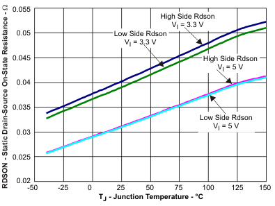 Figure 1. High-Side and Low-Side On-Resistance vs Junction Temperature
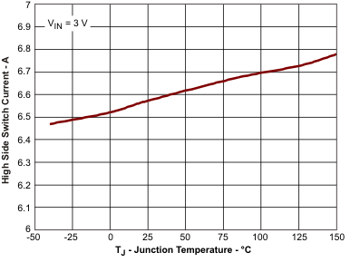 Figure 3. High-Side Current Limit vs Junction Temperature
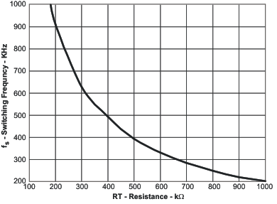 Figure 5. Switching Frequency vs RT Resistance Low Frequency Range
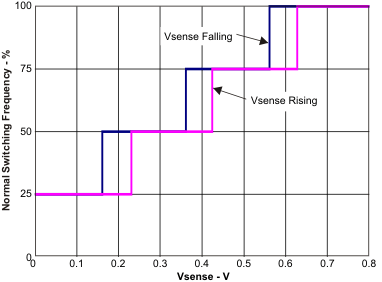 Figure 7. Switching Frequency vs Vsense
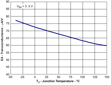 Figure 9. Transconductance (Soft-Start) vs Junction Temperature
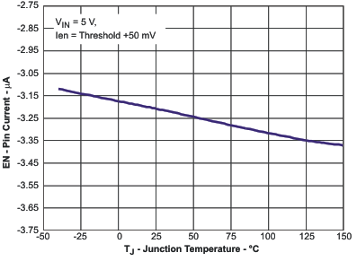 Figure 11. Pin Current vs Junction Temperature
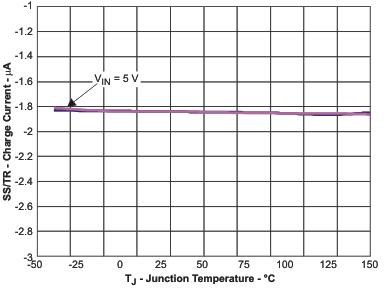 Figure 13. Charge Current vs Junction Temperature
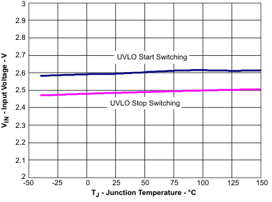 Figure 15. Input Voltage vs Junction Temperature
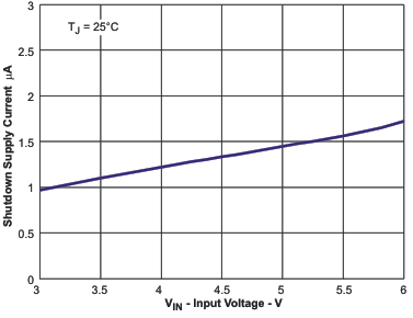 Figure 17. Shutdown Supply Current vs Input Voltage
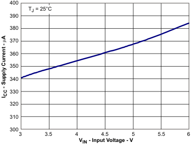 Figure 19. Supply Current vs Input Voltage
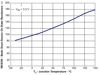 Figure 21. PWRGD On Resistance vs Junction Temperature
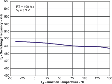 Figure 2. Frequency vs Junction Temperature
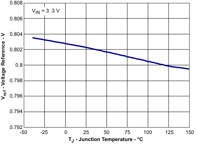 Figure 4. Voltage Reference vs Junction Temperature
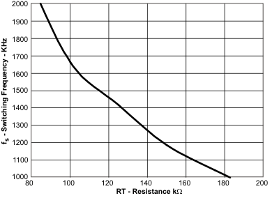 Figure 6. Switching Frequency vs RT Resistance High Frequency Range
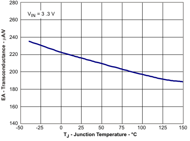 Figure 8. Transconductance vs Junction Temperature
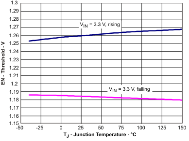 Figure 10. Enable Pin Voltage vs Junction Temperature
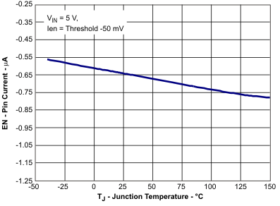 Figure 12. Pin Current vs Junction Temperature
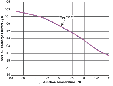 Figure 14. Discharge Current vs Junction Temperature
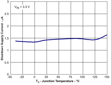 Figure 16. Shutdown Supply Current vs Junction Temperature
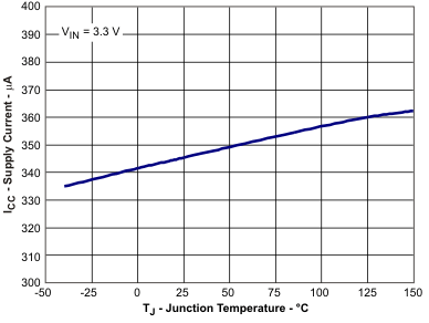 Figure 18. Supply Current vs Junction Temperature
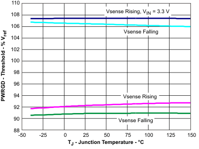 Figure 20. PWRGD Threshold vs Junction Temperature
