ZHCSI04E September 2009 – April 2018 TPS54418
PRODUCTION DATA.
- 1 特性
- 2 应用
- 3 说明
- 4 修订历史记录
- 5 Pin Configuration and Functions
- 6 Specifications
-
7 Detailed Description
- 7.1 Overview
- 7.2 Functional Block Diagram
- 7.3
Feature Description
- 7.3.1 Fixed Frequency PWM Control
- 7.3.2 Slope Compensation and Output Current
- 7.3.3 Bootstrap Voltage (Boot) and Low Dropout Operation
- 7.3.4 Error Amplifier
- 7.3.5 Voltage Reference
- 7.3.6 Adjusting the Output Voltage
- 7.3.7 Enable and Adjusting Undervoltage Lockout
- 7.3.8 Soft-Start Pin
- 7.3.9 Sequencing
- 7.3.10 Constant Switching Frequency and Timing Resistor (RT/CLK Pin)
- 7.3.11 Overcurrent Protection
- 7.3.12 Frequency Shift
- 7.3.13 Reverse Overcurrent Protection
- 7.3.14 Synchronize Using the RT/CLK Pin
- 7.3.15 Power Good (PWRGD Pin)
- 7.3.16 Overvoltage Transient Protection
- 7.3.17 Thermal Shutdown
- 7.4 Device Functional Modes
-
8 Application and Implementation
- 8.1 Application Information
- 8.2
Typical Application
- 8.2.1 Design Requirements
- 8.2.2
Detailed Design Procedure
- 8.2.2.1 Step One: Select the Switching Frequency
- 8.2.2.2 Step Two: Select the Output Inductor
- 8.2.2.3 Step Three: Choose the Output Capacitor
- 8.2.2.4 Step Four: Select the Input Capacitor
- 8.2.2.5 Step Five: Minimum Load DC COMP Voltage
- 8.2.2.6 Step Six: Choose the Soft-Start Capacitor
- 8.2.2.7 Step Seven: Select the Bootstrap Capacitor
- 8.2.2.8 Step Eight: Undervoltage Lockout Threshold
- 8.2.2.9 Step Nine: Select Output Voltage and Feedback Resistors
- 8.2.2.10 Step 10: Select Loop Compensation Components
- 8.2.2.11 Power Dissipation Estimate
- 8.2.3 Application Curves
- 9 Power Supply Recommendations
- 10Layout
- 11器件和文档支持
- 12机械、封装和可订购信息
8.2.2.11 Power Dissipation Estimate
Use Equation 43 through Equation 52 to help estimate the device power dissipation under continuous conduction mode (CCM) operation. The power dissipation of the device (PTOT) includes conduction loss (PCOND), dead time loss (PD), switching loss (PSW), gate drive loss (PGD) and supply current loss (PQ).
Equation 43. PCOND= (IOUT)2 × RDS(on)
Equation 44. PD = ƒSW × IOUT × 0.7 × 60 × (10)–9
Equation 45. PD = ƒSW × IOUT × 0.7 × 60 × (10)–9
Equation 46. PSW = 2 × (VIN)2 × ƒSW × IOUT × 0.25 × (10)–9
Equation 47. PSW = 2 × (VIN)2 × ƒSW × IOUT × 0.25 × (10)–9
Equation 48. PGD = 2 × VIN × 3 × (10)–9 × ƒSW
Equation 49. PQ = 350 × (10)–6 × VIN
where
- IOUT is the output current (A)
- RDS(on) is the on-resistance of the high-side MOSFET (Ω)
- VOUT is the output voltage (V)
- VIN is the input voltage (V)
- ƒSW is the switching frequency (Hz)
Equation 50. PTOT = PCOND + PD + PSW + PGD + PQ
For a given ambient temperature,
Equation 51. TJ = TA + RTH × PTOT
For maximum junction temperature (TJ(max) = 150°C)
Equation 52. TA(max) = TJ(max) – RTH × PTOT
where
- PTOT is the total device power dissipation (W)
- TA is the ambient temperature (°C)
- TJ is the junction temperature (°C)
- RTH is the thermal resistance of the package (°C/W)
- TJ(max) is maximum junction temperature (°C)
- TA(max) is maximum ambient temperature (°C)
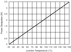
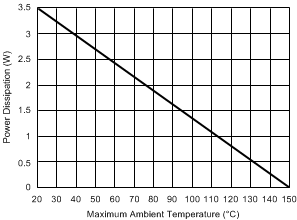
Additional power can be lost in the regulator circuit due to the inductor ac and dc losses and trace resistance that impact the overall regulator efficiency. Figure 36 and Figure 37 show power dissipation for the EVM.

| TA = 25°C | No air flow |

| TJ(max) = 150°C | No air flow |