ZHCSI13J October 2004 – November 2018 TPS75003
PRODUCTION DATA.
- 1 特性
- 2 应用
- 3 说明
- 4 修订历史记录
- 5 Pin Configuration and Functions
- 6 Specifications
-
7 Detailed Description
- 7.1 Overview
- 7.2 Functional Block Diagram
- 7.3
Feature Description
- 7.3.1 Operation (Buck Controllers)
- 7.3.2 Enable (Buck Controllers)
- 7.3.3 UVLO (Buck Controllers)
- 7.3.4 Current Limit (Buck Controllers)
- 7.3.5 Short-Circuit Protection (Buck Controllers)
- 7.3.6 Soft-Start (Buck Controllers)
- 7.3.7 LDO Operation
- 7.3.8 Internal Current Limit (LDO)
- 7.3.9 Enable Pin (LDO)
- 7.3.10 Dropout Voltage (LDO)
- 7.3.11 Transient Response (LDO)
- 7.3.12 Thermal Protection (LDO)
- 7.3.13 Power Dissipation (LDO)
-
8 Application and Implementation
- 8.1 Application Information
- 8.2
Typical Application
- 8.2.1 Design Requirements
- 8.2.2
Detailed Design Procedure
- 8.2.2.1 Input Capacitor CIN1, CIN2 Selection (Buck Controllers)
- 8.2.2.2 Inductor Value Selection (Buck Controllers)
- 8.2.2.3 External PMOS Transistor Selection (Buck Controllers)
- 8.2.2.4 Diode Selection (Buck Controllers)
- 8.2.2.5 Output Capacitor Selection (Buck Controllers)
- 8.2.2.6 Output Voltage Ripple Effect on VOUT (Buck Controllers)
- 8.2.2.7 Soft-Start Capacitor Selection (Buck Controllers)
- 8.2.2.8 Output Voltage Setting Selection (Buck Controllers)
- 8.2.2.9 Input Capacitor Selection (LDO)
- 8.2.2.10 Output Capacitor Selection (LDO)
- 8.2.2.11 Soft-Start Capacitor Selection (LDO)
- 8.2.2.12 Setting Output Voltage (LDO)
- 8.2.3 Application Curves
- 9 Power Supply Recommendations
- 10Layout
- 11器件和文档支持
- 12机械、封装和可订购信息
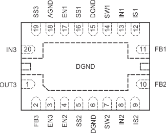
5 Pin Configuration and Functions
RHL Package
20-Pin VQFN
Top View

Pin Functions
| PIN | TYPE | DESCRIPTION | |
|---|---|---|---|
| NAME | NO. | ||
| AGND | 18 | GND | Ground connection for LDO. |
| DGND | 6, 15, PAD | GND | Ground connection for BUCK1 and BUCK2 converters. Pins 6 and 15 should be connected to the back side exposed pad by a short metal trace as shown in the PCB Layout Considerations section of this data sheet. |
| EN1 | 17 | I | Driving the enable pin (ENx) high turns on BUCK1 regulator. Driving this pin low puts it into shutdown mode, reducing operating current. The enable pin does not trigger on fast negative going transients. |
| EN2 | 4 | I | Same as EN1 but for BUCK2 controller. |
| EN3 | 3 | I | Same as EN1 but for LDO. |
| FB1 | 11 | I (Analog) | Feedback pin. Used to set the output voltage of BUCK1 regulator. |
| FB2 | 10 | I (Analog) | Same as FB1 but for BUCK2 controller. |
| FB3 | 2 | I (Analog) | Same as FB1 but for LDO. |
| IN1 | 13 | I (Analog) | Input supply to BUCK1. |
| IN2 | 8 | I (Analog) | Input supply to BUCK2. |
| IN3 | 20 | I (Power) | Input supply to LDO. |
| IS1 | 12 | I (Analog) | Current sense input for BUCK1 regulator. The voltage difference between this pin and IN1 is compared to an internal reference to set current limit. For a robust output start-up ramp, careful layout and bypassing are required. See the Application Information section for details. |
| IS2 | 9 | I (Analog) | Same as IS1 but compared to IN2 and used for BUCK2 controller. |
| OUT3 | 1 | O (Power) | Regulated LDO output. A small ceramic capacitor (≥ 2.2μF) is needed from this pin to ground to ensure stability. |
| SS1 | 16 | I (Analog) | Connecting a capacitor between this pin and ground increases start-up time of the BUCK1 regulator by slowing the ramp-up of current limit. This high-impedance pin is noise-sensitive; careful layout is important. See the Typical Characteristics, Application Information, and PCB Layout Considerations sections for details. |
| SS2 | 5 | I (Analog) | Same as SS1 but for BUCK2 regulator. |
| SS3 | 19 | I (Analog) | Connecting a capacitor from this pin to ground slows the start-up time of the LDO reference, thereby slowing output voltage ramp-up. See the Application Information section for details. |
| SW1 | 14 | O (Analog) | Gate drive pin for external BUCK1 P-channel MOSFET. |
| SW2 | 7 | O (Analog) | Same as SW1 but for BUCK2 controller. |