ZHCSI15L June 2006 – May 2018 TPS65023 , TPS65023B
PRODUCTION DATA.
- 1 特性
- 2 应用
- 3 说明
- 4 修订历史记录
- 5 Pin Configuration and Functions
-
6 Specifications
- 6.1 Absolute Maximum Ratings
- 6.2 ESD Ratings
- 6.3 Recommended Operating Conditions
- 6.4 Thermal Information
- 6.5 Electrical Characteristics
- 6.6 Electrical Characteristics: Supply Pins VCC, VINDCDC1, VINDCDC2, VINDCDC3
- 6.7 Electrical Characteristics: Supply Pins VBACKUP, VSYSIN, VRTC, VINLDO
- 6.8 Electrical Characteristics: VDCDC1 Step-Down Converter
- 6.9 Electrical Characteristics: VDCDC2 Step-Down Converter
- 6.10 Electrical Characteristics: VDCDC3 Step-Down Converter
- 6.11 I2C Timing Requirements for TPS65023B
- 6.12 Typical Characteristics
-
7 Detailed Description
- 7.1 Overview
- 7.2 Functional Block Diagram
- 7.3
Feature Description
- 7.3.1 VRTC Output and Operation With or Without Backup Battery
- 7.3.2 Step-Down Converters, VDCDC1, VDCDC2, and VDCDC3
- 7.3.3 Power Save Mode Operation
- 7.3.4 Low Ripple Mode
- 7.3.5 Soft-Start
- 7.3.6 100% Duty Cycle Low Dropout Operation
- 7.3.7 Active Discharge When Disabled
- 7.3.8 Power-Good Monitoring
- 7.3.9 Low-Dropout Voltage Regulators
- 7.3.10 Undervoltage Lockout
- 7.3.11 Power-Up Sequencing
- 7.4 Device Functional Modes
- 7.5 Programming
- 7.6
Register Maps
- 7.6.1 VERSION Register Address: 00h (Read Only)
- 7.6.2 PGOODZ Register Address: 01h (Read Only)
- 7.6.3 MASK Register Address: 02h (Read and Write), Default Value: C0h
- 7.6.4 REG_CTRL Register Address: 03h (Read and Write), Default Value: FFh
- 7.6.5 CON_CTRL Register Address: 04h (Read and Write), Default Value: B1h
- 7.6.6 CON_CTRL2 Register Address: 05h (Read and Write), Default Value: 40h
- 7.6.7 DEFCORE Register Address: 06h (Read and Write), Default Value: 14h/1Eh
- 7.6.8 DEFSLEW Register Address: 07h (Read and Write), Default Value: 06h
- 7.6.9 LDO_CTRL Register Address: 08h (Read and Write), Default Value: Set with DEFLDO1 and DEFLDO2
- 8 Application and Implementation
- 9 Power Supply Recommendations
- 10Layout
- 11器件和文档支持
- 12机械、封装和可订购信息
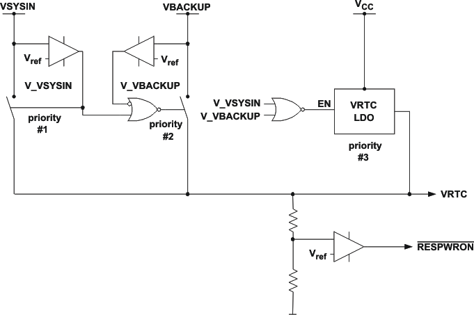
7.3.1 VRTC Output and Operation With or Without Backup Battery
The VRTC pin is an always-on output, intended to supply up to 30 mA to a permanently required rail (that is, for a real time clock). The TPS65023x asserts the RESPWRON signal if VRTC drops below 2.4 V. VRTC is selected from a priority scheme based on the VSYSIN and VBACKUP inputs.
When the voltage at the VSYSIN pin exceeds 2.65 V, VRTC connects to the VSYSIN input through a PMOS switch and all other paths to VRTC are disabled. The PMOS switch drops a maximum of 375 mV at 30 mA, which must be considered when using VRTC. VSYSIN can be connected to any voltage source with the appropriate input voltage, including VCC or, if set to 3.3-V output, DCDC2 or DCDC3. When VSYSIN falls below 2.65 V or shorts to ground, the PMOS switch connecting VRTC and VSYSIN opens and VRTC then connects to either VBACKUP or the output of a dedicated 3-V or 30-mA LDO.
NOTE
Texas Instruments recommends connecting VSYSIN to VCC or ground – VCC if a non-replaceable primary cell is connected to VBACKUP and ground if the VRTC output will float.
If the PMOS switch between VSYSIN and VRTC is open and VBACKUP exceeds 2.65 V, VRTC connects to VBACKUP through a PMOS switch. The PMOS switch drops a maximum of 375 mV at 30 mA, which must be considered if using VRTC. A typical application may connect VBACKUP to a primary Li button cell, but any battery that provides a voltage between 2.65 V and 6 V (that is, a single Li-Ion cell or a single boosted NiMH battery) is acceptable, to supply the VRTC output.
NOTE
In systems with no backup battery, the VBACKUP pin must be connected to GND.
If the switches between VRTC and VSYSIN or VBACKUP are open, the dedicated 3-V or 30-mA LDO, driven from VCC, connects to VRTC. This LDO is disabled if the voltage at the VSYSIN input exceeds 2.65 V.
Inside TPS65023x there is a switch (Vmax switch) which selects the higher voltage between VCC and VBACKUP. This is used as the supply voltage for some basic functions. The functions powered from the output of the Vmax switch are:
- INT output
- RESPWRON output
- HOT_RESET input
- LOW_BATT output
- PWRFAIL output
- Enable pins for DC-DC converters, LDO1 and LDO2
- Undervoltage lockout comparator (UVLO)
- Reference system with low frequency timing oscillators
- LOW_BATT and PWRFAIL comparators
The main 2.25-MHz oscillator, and the I2C interface are only powered from VCC.
