ZHCSI15L June   2006  – May 2018 TPS65023 , TPS65023B

PRODUCTION DATA.  

  1. 特性
  2. 应用
  3. 说明
    1.     简化原理图
  4. 修订历史记录
  5. Pin Configuration and Functions
    1.     Pin Functions
  6. Specifications
    1. 6.1  Absolute Maximum Ratings
    2. 6.2  ESD Ratings
    3. 6.3  Recommended Operating Conditions
    4. 6.4  Thermal Information
    5. 6.5  Electrical Characteristics
    6. 6.6  Electrical Characteristics: Supply Pins VCC, VINDCDC1, VINDCDC2, VINDCDC3
    7. 6.7  Electrical Characteristics: Supply Pins VBACKUP, VSYSIN, VRTC, VINLDO
    8. 6.8  Electrical Characteristics: VDCDC1 Step-Down Converter
    9. 6.9  Electrical Characteristics: VDCDC2 Step-Down Converter
    10. 6.10 Electrical Characteristics: VDCDC3 Step-Down Converter
    11. 6.11 I2C Timing Requirements for TPS65023B
    12. 6.12 Typical Characteristics
  7. Detailed Description
    1. 7.1 Overview
    2. 7.2 Functional Block Diagram
    3. 7.3 Feature Description
      1. 7.3.1  VRTC Output and Operation With or Without Backup Battery
      2. 7.3.2  Step-Down Converters, VDCDC1, VDCDC2, and VDCDC3
      3. 7.3.3  Power Save Mode Operation
      4. 7.3.4  Low Ripple Mode
      5. 7.3.5  Soft-Start
      6. 7.3.6  100% Duty Cycle Low Dropout Operation
      7. 7.3.7  Active Discharge When Disabled
      8. 7.3.8  Power-Good Monitoring
      9. 7.3.9  Low-Dropout Voltage Regulators
      10. 7.3.10 Undervoltage Lockout
      11. 7.3.11 Power-Up Sequencing
    4. 7.4 Device Functional Modes
    5. 7.5 Programming
      1. 7.5.1 System Reset + Control Signals
        1. 7.5.1.1 DEFLDO1 and DEFLDO2
        2. 7.5.1.2 Interrupt Management and the INT Pin
      2. 7.5.2 Serial Interface
    6. 7.6 Register Maps
      1. 7.6.1 VERSION Register Address: 00h (Read Only)
      2. 7.6.2 PGOODZ Register Address: 01h (Read Only)
      3. 7.6.3 MASK Register Address: 02h (Read and Write), Default Value: C0h
      4. 7.6.4 REG_CTRL Register Address: 03h (Read and Write), Default Value: FFh
      5. 7.6.5 CON_CTRL Register Address: 04h (Read and Write), Default Value: B1h
      6. 7.6.6 CON_CTRL2 Register Address: 05h (Read and Write), Default Value: 40h
      7. 7.6.7 DEFCORE Register Address: 06h (Read and Write), Default Value: 14h/1Eh
      8. 7.6.8 DEFSLEW Register Address: 07h (Read and Write), Default Value: 06h
      9. 7.6.9 LDO_CTRL Register Address: 08h (Read and Write), Default Value: Set with DEFLDO1 and DEFLDO2
  8. Application and Implementation
    1. 8.1 Application Information
      1. 8.1.1 Input Voltage Connection
      2. 8.1.2 Unused Regulators
      3. 8.1.3 Reset Condition of DCDC1
    2. 8.2 Typical Application
      1. 8.2.1 Design Requirements
      2. 8.2.2 Detailed Design Procedure
        1. 8.2.2.1 Inductor Selection for the DC-DC Converters
        2. 8.2.2.2 Output Capacitor Selection
        3. 8.2.2.3 Input Capacitor Selection
        4. 8.2.2.4 Output Voltage Selection
        5. 8.2.2.5 VRTC Output
        6. 8.2.2.6 LDO1 and LDO2
        7. 8.2.2.7 TRESPWRON
        8. 8.2.2.8 VCC Filter
      3. 8.2.3 Application Curves
  9. Power Supply Recommendations
    1. 9.1 Requirements for Supply Voltages Below 3.0 V
  10. 10Layout
    1. 10.1 Layout Guidelines
    2. 10.2 Layout Example
  11. 11器件和文档支持
    1. 11.1 器件支持
      1. 11.1.1 第三方米6体育平台手机版_好二三四免责声明
      2. 11.1.2 开发支持
    2. 11.2 文档支持
      1. 11.2.1 相关文档
    3. 11.3 相关链接
    4. 11.4 社区资源
    5. 11.5 商标
    6. 11.6 静电放电警告
    7. 11.7 术语表
  12. 12机械、封装和可订购信息

Pin Configuration and Functions

RSB Package
40-Pin WQFN
Top View
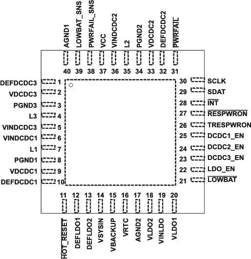
TPS65023 TPS65023B pin_out_lvs613.gif

Pin Functions

PIN I/O DESCRIPTION
NAME NO.
SWITCHING REGULATOR SECTION
AGND1 40 Analog ground. All analog ground pins are connected internally on the chip.
AGND2 17 Analog ground. All analog ground pins are connected internally on the chip.
DCDC1_EN 25 I VDCDC1 enable pin. A logic high enables the regulator, a logic low disables the regulator.
DCDC2_EN 24 I VDCDC2 enable pin. A logic high enables the regulator, a logic low disables the regulator.
DCDC3_EN 23 I VDCDC3 enable pin. A logic high enables the regulator, a logic low disables the regulator.
DEFDCDC1 10 I Input signal indicating default VDCDC1 voltage, 0 = 1.2 V, 1 = 1.6 V DEFDCDC1 can also be connected to a resistor divider between VDCDC1 and GND, if the output voltage of the DCDC1 converter is set in a range from 0.6 V to VINDCDC1 V.
DEFDCDC2 32 I Input signal indicating default VDCDC2 voltage, 0 = 1.8 V, 1 = 3.3 V DEFDCDC2 can also be connected to a resistor divider between VDCDC2 and GND, if the output voltage of the DCDC2 converter is set in a range from 0.6 V to VINDCDC2 V.
DEFDCDC3 1 I Input signal indicating default VDCDC3 voltage, 0 = 1.8 V, 1 = 3.3 V DEFDCDC3 can also be connected to a resistor divider between VDCDC3 and GND, if the output voltage of the DCDC3 converter is set in a range from 0.6 V to VINDCDC3 V.
L1 7 Switch pin of VDCDC1 converter. The VDCDC1 inductor is connected here.
L2 35 Switch pin of VDCDC2 converter. The VDCDC2 inductor is connected here.
L3 4 Switch pin of VDCDC3 converter. The VDCDC3 inductor is connected here.
PGND1 8 Power ground for VDCDC1 converter
PGND2 34 Power ground for VDCDC2 converter
PGND3 3 Power ground for VDCDC3 converter
VCC 37 I Power supply for digital and analog circuitry of VDCDC1, VDCDC2, and VDCDC3 DC-DC converters. VCC must be connected to the same voltage supply as VINDCDC3, VINDCDC1, and VINDCDC2. VCC also supplies serial interface block.
VDCDC1 9 I VDCDC1 feedback voltage sense input. Connect directly to VDCDC1
VDCDC2 33 I VDCDC2 feedback voltage sense input. Connect directly to VDCDC2
VDCDC3 2 I VDCDC3 feedback voltage sense input. Connect directly to VDCDC3
VINDCDC1 6 I Input voltage for VDCDC1 step-down converter. VINDCDC1 must be connected to the same voltage supply as VINDCDC2, VINDCDC3, and VCC.
VINDCDC2 36 I Input voltage for VDCDC2 step-down converter. VINDCDC2 must be connected to the same voltage supply as VINDCDC1, VINDCDC3, and VCC.
VINDCDC3 5 I Input voltage for VDCDC3 step-down converter. VINDCDC3 must be connected to the same voltage supply as VINDCDC1, VINDCDC2, and VCC.
Thermal Pad Connect the power pad to analog ground
LDO REGULATOR SECTION
DEFLD01 12 I Digital input. DEFLD01 sets the default output voltage of LDO1 and LDO2.
DEFLD02 13 I Digital input. DEFLD02 sets the default output voltage of LDO1 and LDO2.
LDO_EN 22 I Enable input for LDO1 and LDO2. A logic high enables the LDOs and a logic low disables the LDOs.
VBACKUP 15 I Connect the backup battery to this input pin
VINLDO 19 I Input voltage for LDO1 and LDO2
VLDO1 20 O Output voltage of LDO1
VLDO2 18 O Output voltage of LDO2
VRTC 16 O Output voltage of the LDO and switch for the real time clock
VSYSIN 14 I Input of system voltage for VRTC switch
CONTROL AND I2C SECTION
HOT_RESET 11 I Push button input that reboots or wakes up the processor through the RESPWRON output pin.
INT 28 O Open-drain output
LOW_BAT 21 O Open-drain output of LOW_BAT comparator
LOWBAT_SNS 39 I Input for the comparator driving the LOW_BAT output.
PWRFAIL 31 O Open-drain output. Active low when PWRFAIL comparator indicates low VBAT condition.
PWRFAIL_SNS 38 I Input for the comparator driving the PWRFAIL output
RESPWRON 27 O Open-drain system reset output
SCLK 30 I Serial interface clock line
SDAT 29 I/O Serial interface data and address
TRESPWRON 26 I Connect the timing capacitor to TRESPWRON to set the reset delay time: 1 nF → 100 ms