ZHCSI15L June 2006 – May 2018 TPS65023 , TPS65023B
PRODUCTION DATA.
- 1 特性
- 2 应用
- 3 说明
- 4 修订历史记录
- 5 Pin Configuration and Functions
-
6 Specifications
- 6.1 Absolute Maximum Ratings
- 6.2 ESD Ratings
- 6.3 Recommended Operating Conditions
- 6.4 Thermal Information
- 6.5 Electrical Characteristics
- 6.6 Electrical Characteristics: Supply Pins VCC, VINDCDC1, VINDCDC2, VINDCDC3
- 6.7 Electrical Characteristics: Supply Pins VBACKUP, VSYSIN, VRTC, VINLDO
- 6.8 Electrical Characteristics: VDCDC1 Step-Down Converter
- 6.9 Electrical Characteristics: VDCDC2 Step-Down Converter
- 6.10 Electrical Characteristics: VDCDC3 Step-Down Converter
- 6.11 I2C Timing Requirements for TPS65023B
- 6.12 Typical Characteristics
-
7 Detailed Description
- 7.1 Overview
- 7.2 Functional Block Diagram
- 7.3
Feature Description
- 7.3.1 VRTC Output and Operation With or Without Backup Battery
- 7.3.2 Step-Down Converters, VDCDC1, VDCDC2, and VDCDC3
- 7.3.3 Power Save Mode Operation
- 7.3.4 Low Ripple Mode
- 7.3.5 Soft-Start
- 7.3.6 100% Duty Cycle Low Dropout Operation
- 7.3.7 Active Discharge When Disabled
- 7.3.8 Power-Good Monitoring
- 7.3.9 Low-Dropout Voltage Regulators
- 7.3.10 Undervoltage Lockout
- 7.3.11 Power-Up Sequencing
- 7.4 Device Functional Modes
- 7.5 Programming
- 7.6
Register Maps
- 7.6.1 VERSION Register Address: 00h (Read Only)
- 7.6.2 PGOODZ Register Address: 01h (Read Only)
- 7.6.3 MASK Register Address: 02h (Read and Write), Default Value: C0h
- 7.6.4 REG_CTRL Register Address: 03h (Read and Write), Default Value: FFh
- 7.6.5 CON_CTRL Register Address: 04h (Read and Write), Default Value: B1h
- 7.6.6 CON_CTRL2 Register Address: 05h (Read and Write), Default Value: 40h
- 7.6.7 DEFCORE Register Address: 06h (Read and Write), Default Value: 14h/1Eh
- 7.6.8 DEFSLEW Register Address: 07h (Read and Write), Default Value: 06h
- 7.6.9 LDO_CTRL Register Address: 08h (Read and Write), Default Value: Set with DEFLDO1 and DEFLDO2
- 8 Application and Implementation
- 9 Power Supply Recommendations
- 10Layout
- 11器件和文档支持
- 12机械、封装和可订购信息
8.1.3 Reset Condition of DCDC1
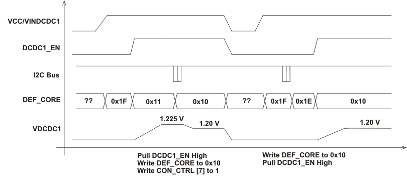
If DEFDCDC1 is connected to ground and DCDC1_EN is pulled high after VINDCDC1 is applied, the output voltage of DCDC1 defaults to 1.225 V instead of 1.2 V (high by 2%). Figure 36 illustrates the problem.
 Figure 36. Default DCDC1
 One workaround is to tie DCDC1_EN to VINDCDC1 (Figure 37).
 Figure 37. Workaround 1
 Another workaround is to write the correct voltage to the DEF_CORE register through I2C. This can be done before or after the converter is enabled. If written before the enable, the only bit changed is DEF_CORE[0]. The voltage is 1.2 V, however, when the enable is pulled high (Figure 38).
 Figure 38. Workaround 2
 A third workaround is to generate a HOT_RESET after enabling DCDC1 (Figure 39)
 Figure 39. Workaround 3
 Table 17. Changes of TPS65023B vs TPS65023
| ITEM | DESCRIPTION | Reference | TPS65023 | TPS65023B |
|---|---|---|---|---|
| VIH | High level input voltage for the SDAT pin | Electrical Characteristics | Minimum 1.3 V | Minimum 1.69 V;
Vcc = 2.5 V to 5.25 V Minimum 1.55 V; Vcc = 2.5 V to 4.5 V |
| VIH | High level input voltage for the SCLK pin | Minimum 1.3 V | Minimum 1.4 V;
Vcc = 2.5 V to 5.25 V |
|
| VIL | Low level input voltage for SCLK and SDAT pin | Maximum 0.4 V | Maximum 0.35 V | |
| th(DATA) | Data input hold time | I2C Timing Requirements for TPS65023B | Minimum 300 ns | Minimum 100 ns |
| tsu(DATA) | Data input setup time | Minimum 300 ns | Minimum 100 ns |