ZHCSI18A April   2018  – July 2018 OPA858

PRODUCTION DATA.  

  1. 特性
  2. 应用
  3. 说明
    1.     Device Images
      1.      高速飞行时间接收器
      2.      光电二极管电容与带宽和噪声
  4. 修订历史记录
  5. Device Comparison Table
  6. Pin Configuration and Functions
    1.     Pin Functions
  7. Specifications
    1. 7.1 Absolute Maximum Ratings
    2. 7.2 ESD Ratings
    3. 7.3 Recommended Operating Conditions
    4. 7.4 Thermal Information
    5. 7.5 Electrical Characteristics
    6. 7.6 Typical Characteristics
  8. Parameter Measurement Information
    1. 8.1 Parameter Measurement Information
  9. Detailed Description
    1. 9.1 Overview
    2. 9.2 Functional Block Diagram
    3. 9.3 Feature Description
      1. 9.3.1 Input and ESD Protection
      2. 9.3.2 Feedback Pin
      3. 9.3.3 Wide Gain-Bandwidth Product
      4. 9.3.4 Slew Rate and Output Stage
      5. 9.3.5 Current Noise
    4. 9.4 Device Functional Modes
      1. 9.4.1 Split-Supply and Single-Supply Operation
      2. 9.4.2 Power-Down Mode
  10. 10Application and Implementation
    1. 10.1 Application Information
      1. 10.1.1 Using the OPA858 as a Transimpedance Amplifier
    2. 10.2 Typical Application
      1. 10.2.1 Design Requirements
      2. 10.2.2 Detailed Design Procedure
      3. 10.2.3 Application Curves
  11. 11Power Supply Recommendations
  12. 12Layout
    1. 12.1 Layout Guidelines
    2. 12.2 Layout Example
  13. 13器件和文档支持
    1. 13.1 接收文档更新通知
    2. 13.2 社区资源
    3. 13.3 商标
    4. 13.4 静电放电警告
    5. 13.5 术语表
  14. 14机械、封装和可订购信息

Typical Characteristics

VS+ = 2.5 V, VS– = –2.5 V, VIN+ = 0 V, RF = 453 Ω, Gain = 7 V/V, RL = 200 Ω, output load referenced to midsupply, and TA = 25°C (unless otherwise noted)
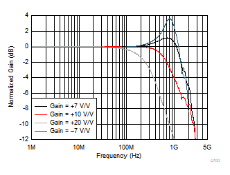
OPA858 D100_SBOS629.gif
VOUT = 100 mVPP; see Figure 43 and Figure 44 for circuit configuration
Figure 1. Small-Signal Frequency Response vs Gain
OPA858 D103_SBOS629.gif
VOUT = 100 mVPP
Figure 3. Small-Signal Frequency Response vs Output Load
OPA858 D105_SBOS629.gif
VOUT = 100 mVPP; see Figure 45 for circuit configuration
Figure 5. Small-Signal Frequency Response vs Capacitive Load
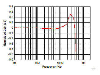
OPA858 D107_SBOS629.gif
VOUT = 2 VPP
Figure 7. Large-Signal Response for 0.1-dB Gain Flatness
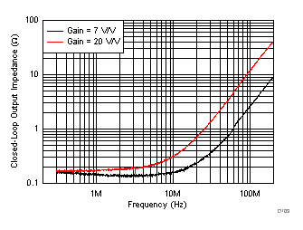
OPA858 D109_SBOS629.gif
Small-Signal Response
Figure 9. Closed-Loop Output Impedance vs Frequency
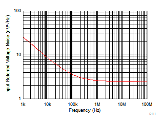
OPA858 D111_SBOS629.gif
Figure 11. Voltage Noise Density vs Frequency
OPA858 D113_SBOS629.gif
Figure 13. Harmonic Distortion (HD2) vs Output Swing
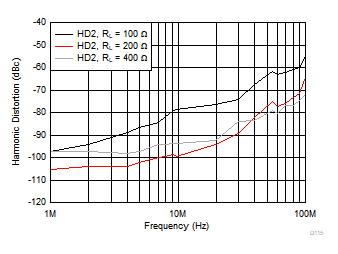
OPA858 D115_SBOS629.gif
VOUT = 2 VPP
Figure 15. Harmonic Distortion (HD2) vs Output Load
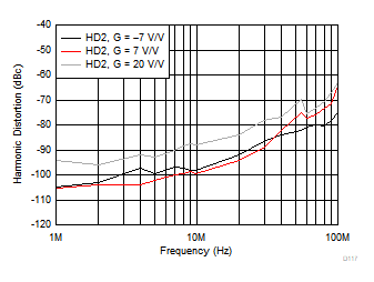
OPA858 D117_SBOS629.gif
VOUT = 2 VPP
Figure 17. Harmonic Distortion (HD2) vs Gain
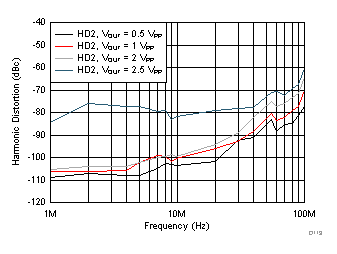
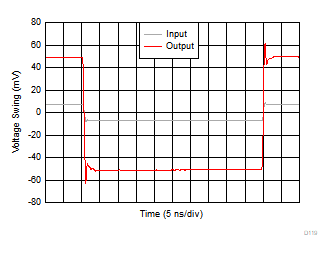
OPA858 D119_SBOS629.gif
Average Rise and Fall Time (10% - 90%) = 450 ps
Figure 19. Small-Signal Transient Response
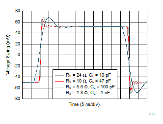
OPA858 D121_SBOS629.gif
Figure 21. Small-Signal Transient Response vs Capacitive Load
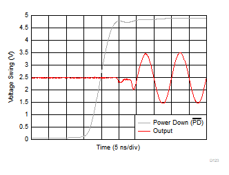
OPA858 D123_SBOS629.gif
VS+ = 5 V, VS– = Ground
Figure 23. Turnon Transient Response
OPA858 D125_SBOS629.gif
Small-Signal Response
Figure 25. Common-Mode Rejection Ratio vs Frequency
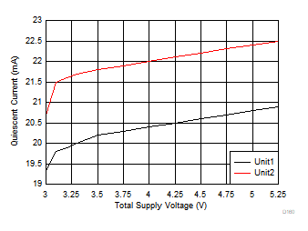
OPA858 D160_SBOS629.gif
2 Typical Units
Figure 27. Quiescent Current vs Supply Voltage
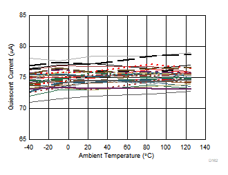
OPA858 D162_SBOS629.gif
30 Units Tested
Figure 29. Quiescent Current (Amplifier Disabled) vs Ambient Temperature
OPA858 D164_SBOS629.gif
µ = 1 µV/°C σ = 2.2 µV/°C 28 Units Tested
Figure 31. Offset Voltage vs Ambient Temperature
OPA858 D166_SBOS629.gif
VS = 5 V 3 Typical Units
Figure 33. Offset Voltage vs Input Common-Mode Voltage
OPA858 D168_SBOS629.gif
VS = 3.3 V 3 Typical Units
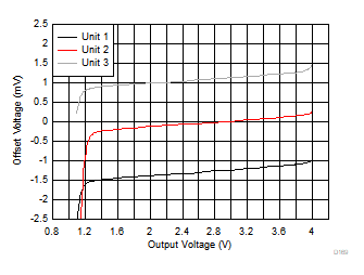
Figure 35. Offset Voltage vs Output Swing
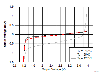
OPA858 D170_SBOS629.gif
Figure 37. Offset Voltage vs Output Swing vs Ambient Temperature
OPA858 D172_SBOS629.gif
Figure 39. Input Bias Current vs Input Common-Mode Voltage
OPA858 D141_SBOS629.gif
µ = –0.28 mV σ = 0.8 mV 4555 units tested
Figure 41. Offset Voltage Distribution
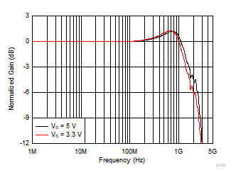
OPA858 D102_SBOS629.gif
VOUT = 100 mVPP
Figure 2. Small-Signal Frequency Response vs Supply Voltage
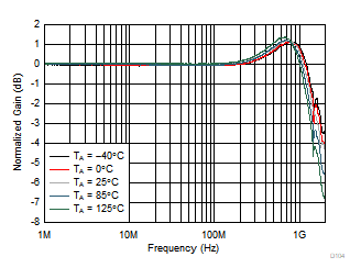
OPA858 D104_SBOS629.gif
VOUT = 100 mVPP
Figure 4. Small-Signal Frequency Response vs Ambient Temperature
OPA858 D106_SBOS629.gif
VOUT = 2 VPP
Figure 6. Large-Signal Frequency Response vs Gain
OPA858 D108_SBOS629.gif
VS = 3.3 V VOUT = 1 VPP
Figure 8. Large-Signal Frequency Response
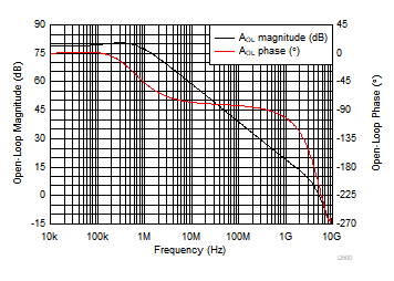
OPA858 D500_SBOS852.gif
Small-Signal Response
Figure 10. Open-Loop Magnitude and Phase vs Frequency
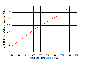
OPA858 D112_SBOS629.gif
Frequency = 10 MHz
Figure 12. Voltage Noise Density vs Ambient Temperature
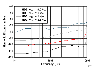
OPA858 D114_SBOS629.gif
Figure 14. Harmonic Distortion (HD3) vs Output Swing
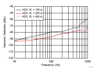
OPA858 D116_SBOS629.gif
VOUT = 2 VPP
Figure 16. Harmonic Distortion (HD3) vs Output Load
OPA858 D118_SBOS629.gif
VOUT = 2 VPP
Figure 18. Harmonic Distortion (HD3) vs Gain
OPA858 D120_SBOS629.gif
Average Rise and Fall Time (10% - 90%) = 750 ps
Figure 20. Large-Signal Transient Response
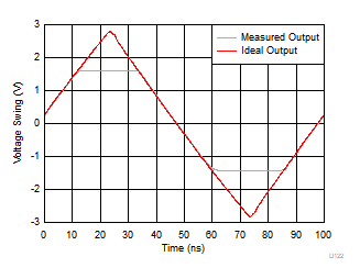
OPA858 D122_SBOS629.gif
2x Output Overdrive
Figure 22. Output Overload Response
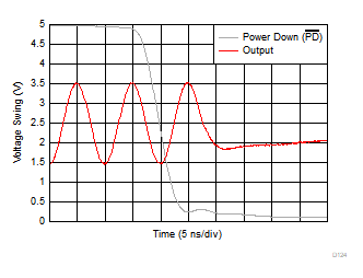
OPA858 D124_SBOS629.gif
VS+ = 5 V, VS– = Ground
Figure 24. Turnoff Transient Response
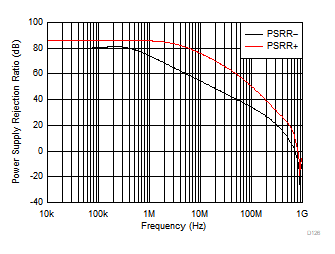
OPA858 D126_SBOS629.gif
Small-Signal Response
Figure 26. Power Supply Rejection Ratio vs Frequency
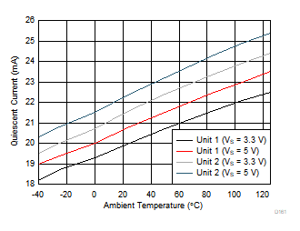
OPA858 D161_SBOS629.gif
2 Typical Units
Figure 28. Quiescent Current vs Ambient Temperature
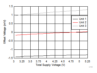
OPA858 D163_SBOS629.gif
3 Typical Units
Figure 30. Offset Voltage vs Supply Voltage
OPA858 D165_SBOS629.gif
VS = 3.3 V 3 Typical Units
Figure 32. Offset Voltage vs Input Common-Mode Voltage
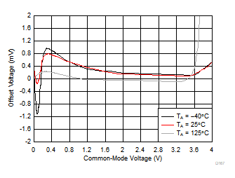
OPA858 D167_SBOS629.gif
Figure 34. Offset Voltage vs Input Common-Mode Voltage vs Ambient Temperature
OPA858 D169_SBOS629.gif
VS = 5 V 3 Typical Units
Figure 36. Offset Voltage vs Output Swing
OPA858 D171_SBOS629.gif
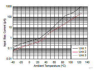
3 Typical Units
Figure 38. Input Bias Current vs Ambient Temperature
OPA858 D140_SBOS629.gif
µ = 20.35 mA σ = 0.2 mA 4555 units tested
Figure 40. Quiescent Current Distribution
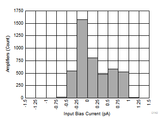
OPA858 D142_SBOS629.gif
µ = –0.1 pA σ = 0.39 pA 4555 units tested
Figure 42. Input Bias Current Distribution