ZHCSI18A April   2018  – July 2018 OPA858

PRODUCTION DATA.  

  1. 特性
  2. 应用
  3. 说明
    1.     Device Images
      1.      高速飞行时间接收器
      2.      光电二极管电容与带宽和噪声
  4. 修订历史记录
  5. Device Comparison Table
  6. Pin Configuration and Functions
    1.     Pin Functions
  7. Specifications
    1. 7.1 Absolute Maximum Ratings
    2. 7.2 ESD Ratings
    3. 7.3 Recommended Operating Conditions
    4. 7.4 Thermal Information
    5. 7.5 Electrical Characteristics
    6. 7.6 Typical Characteristics
  8. Parameter Measurement Information
    1. 8.1 Parameter Measurement Information
  9. Detailed Description
    1. 9.1 Overview
    2. 9.2 Functional Block Diagram
    3. 9.3 Feature Description
      1. 9.3.1 Input and ESD Protection
      2. 9.3.2 Feedback Pin
      3. 9.3.3 Wide Gain-Bandwidth Product
      4. 9.3.4 Slew Rate and Output Stage
      5. 9.3.5 Current Noise
    4. 9.4 Device Functional Modes
      1. 9.4.1 Split-Supply and Single-Supply Operation
      2. 9.4.2 Power-Down Mode
  10. 10Application and Implementation
    1. 10.1 Application Information
      1. 10.1.1 Using the OPA858 as a Transimpedance Amplifier
    2. 10.2 Typical Application
      1. 10.2.1 Design Requirements
      2. 10.2.2 Detailed Design Procedure
      3. 10.2.3 Application Curves
  11. 11Power Supply Recommendations
  12. 12Layout
    1. 12.1 Layout Guidelines
    2. 12.2 Layout Example
  13. 13器件和文档支持
    1. 13.1 接收文档更新通知
    2. 13.2 社区资源
    3. 13.3 商标
    4. 13.4 静电放电警告
    5. 13.5 术语表
  14. 14机械、封装和可订购信息

Feedback Pin

The OPA858 pin layout is optimized to minimize parasitic inductance and capacitance, which is critical in high-speed analog design. The FB pin (pin 1) is internally connected to the output of the amplifier. The FB pin is separated from the inverting input of the amplifier (pin 3) by a no connect (NC) pin (pin 2). The NC pin must be left floating. There are two advantages to this pin layout:

  1. A feedback resistor (RF) can connect between the FB and IN– pin on the same side of the package (see Figure 49) rather than going around the package.
  2. The isolation created by the NC pin minimizes the capacitive coupling between the FB and IN– pins by increasing the physical separation between the pins.
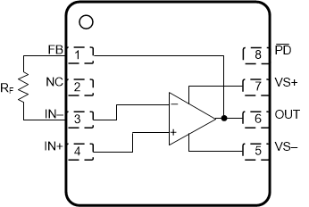
OPA858 OPA85X_FB-Pin.gifFigure 49. RF Connection Between FB and IN– Pins