ZHCSI18A April 2018 – July 2018 OPA858
PRODUCTION DATA.
10.1.1 Using the OPA858 as a Transimpedance Amplifier
The OPA858 design has been optimized to meet the industry's growing demand for wideband, low-noise photodiode amplifiers. The closed-loop bandwidth of a transimpedance amplifier is a function of the following:
- The total input capacitance. This includes the photodiode capacitance, input capacitance of the amplifier (common-mode and differential capacitance) and any stray capacitance from the PCB.
- The op amp gain bandwidth product (GBWP), and,
- The transimpedance gain RF.
 Figure 56. Transimpedance Amplifier Circuit
 Figure 56 shows the OPA858 configured as a TIA with the avalanche photodiode (APD) reverse biased such that its cathode is tied to a large positive bias voltage. In this configuration the APD sources current into the op amp feedback loop so that the output swings in a negative direction relative to the input common-mode voltage. To maximize the output swing in the negative direction, the OPA858 common-mode is set close to the positive limit, 1.6 V from the positive supply rail.
The feedback resistance RF and the input capacitance form a zero in the noise gain that results in instability if left unchecked. To counteract the effect of the zero, a pole is inserted by adding the feedback capacitor (CF.) into the noise gain transfer function. The Transimpedance Considerations for High-Speed Amplifiers application report discusses theories and equations that show how to compensate a transimpedance amplifier for a particular gain and input capacitance. The bandwidth and compensation equations from the application report are available in a Microsoft Excel ™ calculator. What You Need To Know About Transimpedance Amplifiers – Part 1 provides a link to the calculator.
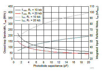
 Figure 57. Bandwidth and Noise Performance vs Photodiode Capacitance
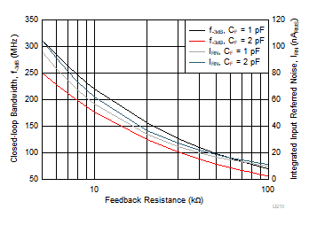
  Figure 58. Bandwidth and Noise Performance vs Feedback Resistance
 The equations and calculators in the application report and blog posts referenced above are used to model the bandwidth (f-3dB) and noise (IRN) performance of the OPA858 configured as a TIA. The resultant performance is shown in Figure 57 and Figure 58. The left side Y-axis shows the closed-loop bandwidth performance, while the right side of the graph shows the integrated input referred noise. The noise bandwidth to calculate IRN, for a fixed RF and CPD is set equal to the f–3dB frequency.
Figure 57 shows the amplifier performance as a function of photodiode capacitance (CPD) for RF = 10 kΩ and 20 kΩ. Increasing CPD decreases the closed-loop bandwidth. It is vital to reduce any stray parasitic capacitance from the PCB to maximize bandwidth. The OPA858 is designed with 0.8 pF of total input capacitance to minimize the effect on system performance.
Figure 58 shows the amplifier performance as a function of RF for CPD = 1 pF and 2 pF. Increasing RF results in lower bandwidth. To maximize the signal-to-noise ratio (SNR) in an optical front-end system, maximize the gain in the TIA stage. Increasing RF by a factor of "X" increases the signal level by "X", but only increases the resistor noise contribution by "√X", thereby improving SNR.