ZHCSI23B April   2018  – March 2020 TLV62568A , TLV62569A

PRODUCTION DATA.  

  1. 特性
  2. 应用
  3. 说明
    1.     Device Images
      1.      sp sp sp典型应用原理图
      2.      sp sp在 5V 输入电压下的效率
  4. 修订历史记录
  5. Pin Configuration and Functions
    1.     Pin Functions
  6. Specifications
    1. 6.1 Absolute Maximum Ratings
    2. 6.2 ESD Ratings
    3. 6.3 Recommended Operating Conditions
    4. 6.4 Thermal Information
    5. 6.5 Electrical Characteristics
    6. 6.6 Typical Characteristics
  7. Detailed Description
    1. 7.1 Overview
    2. 7.2 Functional Block Diagrams
    3. 7.3 Feature Description
      1. 7.3.1 100% Duty Cycle Low Dropout Operation
      2. 7.3.2 Soft Startup
      3. 7.3.3 Switch Current Limit
      4. 7.3.4 Under Voltage Lockout
      5. 7.3.5 Thermal Shutdown
    4. 7.4 Device Functional Modes
      1. 7.4.1 Enabling/Disabling the Device
      2. 7.4.2 Power Good
  8. Application and Implementation
    1. 8.1 Application Information
    2. 8.2 Typical Application
      1. 8.2.1 Design Requirements
      2. 8.2.2 Detailed Design Procedure
        1. 8.2.2.1 Custom Design With WEBENCH® Tools
        2. 8.2.2.2 Setting the Output Voltage
        3. 8.2.2.3 Output Filter Design
        4. 8.2.2.4 Inductor Selection
        5. 8.2.2.5 Input and Output Capacitor Selection
      3. 8.2.3 Application Performance Curves
  9. Power Supply Recommendations
  10. 10Layout
    1. 10.1 Layout Guidelines
    2. 10.2 Layout Example
    3. 10.3 Thermal Considerations
  11. 11器件和文档支持
    1. 11.1 器件支持
      1. 11.1.1 第三方米6体育平台手机版_好二三四免责声明
      2. 11.1.2 开发支持
        1. 11.1.2.1 使用 WEBENCH® 工具创建定制设计
    2. 11.2 文档支持
      1. 11.2.1 相关文档
    3. 11.3 接收文档更新通知
    4. 11.4 支持资源
    5. 11.5 商标
    6. 11.6 静电放电警告
    7. 11.7 Glossary
  12. 12机械、封装和可订购信息

Application Performance Curves

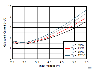
VIN = 5 V, VOUT = 1.8 V, TA = 25 °C, external components shown in Table 3, unless otherwise noted.
TLV62568A TLV62569A D001-SLVSE95_TLV62569A-01.gif
VOUT = 0.6 V
Figure 7. Quiescent Current
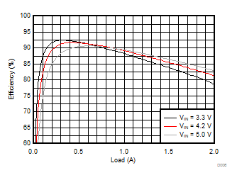
TLV62568A TLV62569A D006-SLVSE95_TLV62569A-01.gif
Figure 9. 1.2-V Output Efficiency
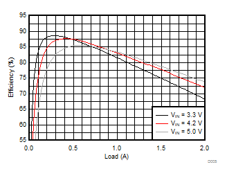
TLV62568A TLV62569A D005-SLVSE95_TLV62569A-01.gif
Figure 8. 0.6-V Output Efficiency
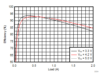
TLV62568A TLV62569A D004-SLVSE95_TLV62569A-01.gif
Figure 10. 1.8-V Output Efficiency
TLV62568A TLV62569A D023-SLVSE95_TLV62569A-01.gif
Figure 11. 2.5-V Output Efficiency
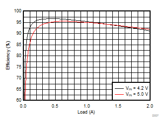
TLV62568A TLV62569A D008-SLVSE95_TLV62569A-01.gif
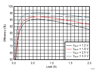
Figure 13. 5.0-V Input Efficiency
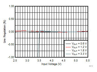
TLV62568A TLV62569A D010-SLVSE95_TLV62569A-01.gif
IOUT = 1 A
Figure 15. Line Regulation
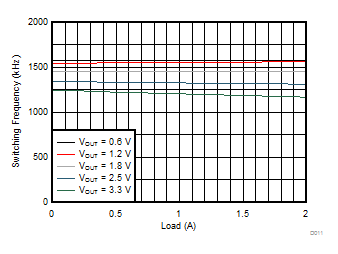
TLV62568A TLV62569A D011-SLVSE95_TLV62569A-01.gif
VIN = 5 V
Figure 17. Switching Frequency vs Load
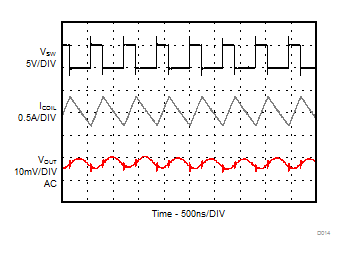
TLV62568A TLV62569A D014-SLVSE95-TLV62569A.gif
IOUT = 36 mA
Figure 19. PWM Operation
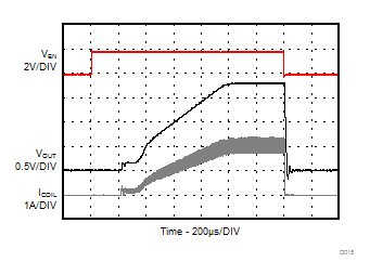
TLV62568A TLV62569A D015-SLVSE95-TLV62569A.gif
Load = 0.9 Ω
Figure 21. Startup and Shutdown with Load
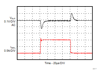
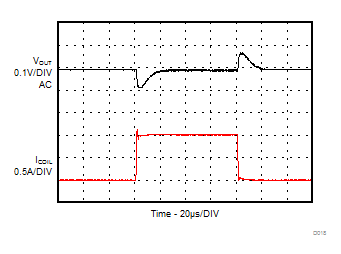
TLV62568A TLV62569A D017-SLVSE95-TLV62569A.gif
Load Step 0 A to 1 A, 1A/μs slew rate
Figure 23. Load Transient
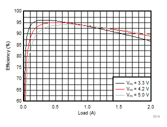
TLV62568A TLV62569A D007-SLVSE95_TLV62569A-01.gif
Figure 12. 3.3-V Output Efficiency
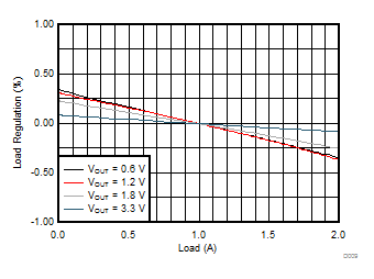
TLV62568A TLV62569A D009-SLVSE95_TLV62569A-01.gif
VIN = 5 V
Figure 14. Load Regulation
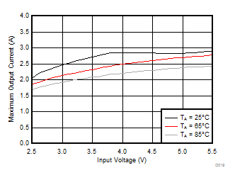
TLV62568A TLV62569A D019-SLVSE95_TLV62569A-01.gif
PG is high
Figure 16. Maximum Output Current at VOUT = 1.8 V
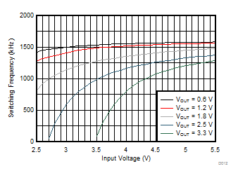
TLV62568A TLV62569A D012-SLVSE95_TLV62569A-01.gif
IOUT = 1 A
Figure 18. Switching Frequency vs Input Voltage
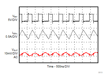
TLV62568A TLV62569A D013-SLVSE95-TLV62569A.gif
IOUT = 1 A
Figure 20. PWM Operation
TLV62568A TLV62569A D016-SLVSE95-TLV62569A.gif
Load = 9 Ω
Figure 22. Startup and Shutdown with Load
TLV62568A TLV62569A D018-SLVSE95-TLV62569A.gif
Load Step 0 A to 1 A, 1A/μs slew rate C3 = 10 pF
Figure 24. Load Transient with A Feed Forward Capacitor